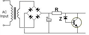
The circuit diagram of transistor shunt regulator is shown in above. the transistor is connected in shunt (parallel) with the load hence the circuit is called transistor shunt regulator. The zener voltage VZ of zener diode is reverse biased by the unregulated DC voltage. To limit the zener current a resistor R1 is connected in series with a zener diode. A transistor Q1 is connected in shunt with the load resistor RL is used as controlling device and its function is to shunt part of the supply current from the load. The transistor must pass the current all the time it is operating, for a shunt regulator to perform a efficiently. It may be noted from the circuit that the load voltage VOut is equal to the sum of zener voltage and the base to emitter voltage VBE of a transistor.
VOut = VZ + VBE OR VBE = VOut -VZ
There is the voltage for given diode is fixed, therefore any increase or decrease in load voltage will have a corresponding effect on the voltage VBE.