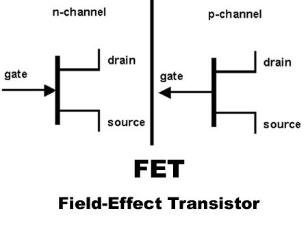
The field effect transistor (FET) is another type of transistor which operates on the principle of that semiconductor conductivity can be increased or decreased by the presence of an electric field.
An electric field can increase the number of free electrons and holes in a semiconductor thus changing its conductivity.
The FET is a three terminal uni-polar solid state device in which the current is by an electric field as in vacuum tubes.
The vacuum tubes are voltage controlled device while the transistors (BJTs) are current control device.
FETs are also called as uni-polar transistor because they involve single carrier type operation. At low frequencies field effect transistor (FET) indicates very high input impedance.
The FETs have three terminals are Source, Drain and Gate.
Source (S): In which the carriers enter the channel. The current entering the channel at is indicated by IS. The drain to source voltage is VGS.
Drain (D): In this carriers leave the channel. The current entering the channel at drain is indicated by ID. The drain to source voltage is VDS.
Gate (G): It is the terminal that modulates the channel conductivity by applying voltage to gate (G) one can control ID.

