- For a regulated power supply, there are many different types of voltage regulators available, such as the 7812 and 7805. But each of these regulators outputs a fixed value. An LM317 IC voltage regulator, which we covered in the last post, is utilized for uneven voltage regulation. The most well-known integrated circuit for voltage regulation is the LM723, and we are now creating a voltage regulation circuit based on it. Basic electronic components like ICs, resistors, and capacitors can be used to build this circuit. For instance, if we use a 9V supply to power this circuit, the regulated supply can be changed using a potentiometer from 4 to 8 volts. The main purpose of using this IC is to provide an extreme amount of current by using an exterior pass transistor. Here the range of the extreme amount of current will be up to 10A.
About LM723?
- The LM723 IC is a switchable voltage regulator that operates in series with a 150mA current output without the necessity of an external pass transistor. When we use an external transistor, the load is driven with 10A of current. The output voltage varies from 3 to 40 volts, while the input voltage source has a maximum of 40 volts.

- The major uses for this IC are as a current regulator and a shunt regulator. Because of its low supply of current drains, which are linear with its working temperature range of -55 °C to 150 °C, this IC can be used for folding back current limiting. The following devices serve as the LM723 IC’s equivalent voltage regulators: MC1723CP, LM723CN, LM723N, LM723QML, and LM723CMX.
Pin Configuration
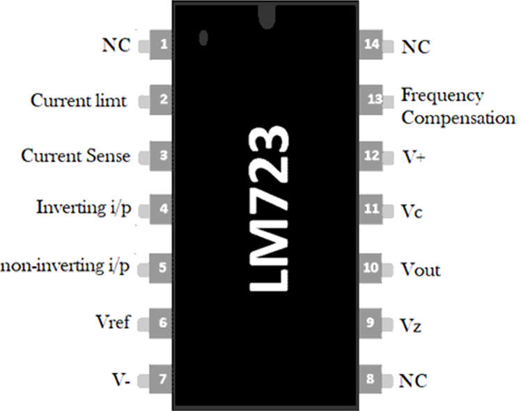
The Pin Configuration of the LM723 and each pin is discussed below.

| Pin No. | Description |
|---|---|
| Pin 1 | NC : Not Connected |
| Pin 2 | Current Limit : This is used to limit the current |
| Pin 3 | Current Sense : This is used in foldback applications as well as to limit the current |
| Pin 4 | Inverting Input : This pin provides stable o/p voltage |
| Pin 5 | Non-Inverting Input : This pin is used to supply a reference voltage to the inside of the operational amplifier |
| Pin 6 | Vref : This pin provides an almost 7v reference voltage |
| Pin 7 | -Vcc : GND (Ground) Pin |
| Pin 8 | NC : Not Connected |
| Pin 9 | Vz : This pin is generally used to make negative regulators |
| Pin 10 | Vout : This is the o/p pin |
| Pin 11 | Vc : This is the series pass transistor’s collector input. Generally, it is connected directly to the +ve voltage supply if an exterior transistor is not used. |
| Pin 12 | V+ : This is the input of the positive supply |
| Pin 13 | Frequency Compensation : This pin assists in decreasing noise with a 100pf capacitor |
| Pin 14 | NC : Not connected |
Features of LM723
- Without utilizing an external pass transistor, the o/p current will be 150mA higher than necessary.
- The input supply voltage will not exceed 40V.
- It has adjustable o/p ranging from 3 to 37 volts.
- To create switching and linear regulators, these ICs are employed.
- With the aid of an external pass transistor, it provides 10A of open-circuit current.
- These ICs are employed in a variety of processes, including positive, negative, series, floating, and shunt operations.
Specifications of LM723
- The maximum i/p voltage is 40v.
- The reference voltage is always 7 volts.
- Ripple rejection is 74 dB.
- The current supply from the Vz pin is 25mA.
- The output voltage ranges from 3volts to 37 volts.
- The range of operating temperature will be from -55°C to +150°C.
- The current supply from the Vref pin is 15mA.
- The line and load regulation of 0.01%Vout & 0.03% Vout.
LM723 Internal Block Diagram
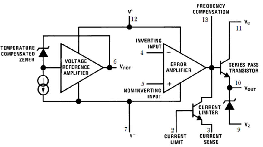
- The internal block diagram of the LM723 IC is shown below. This block diagram can be explained by separating it into two blocks namely the error amplifier and the reference voltage generator.
- In the reference block, a Zener diode is being forced to work at a set point, so the o/p of the more zen is a permanent voltage with a stable current supply which arrives to produce a stable voltage (7.15V) along with an amplifier on the Vref pin of the IC.

- A series pass Q1 transistor, an error amplifier, and a transistor that restricts current are all included in the error amplifier block. By providing feedback to the Vref-reference voltage provided at the non-inverting terminal, this amplifier is utilized to contrast the o/p voltage provided at the inverting i/p terminal.
- The two connections must be provided outside under the required output voltage because they are not available within. The error signal regulates the conduction of the transistor Q1. This transistor is in charge of managing the output voltage.
Advantages of LM723 Voltage Regulator
- The advantages of the LM723 voltage regulator include proven, low noise, the voltage range is wide, support for external pass transistors, recompense by the user, extremely flexible, complete temperature range accessible, and economical.
Disadvantages of LM723 Voltage Regulator
- The disadvantages of LM723 voltage regulator include difficulty, current limiting is not exact, current limiting is sensitive to overload, lowest dropout voltage, least regulated o/p voltage, error amplifier gain is Moderate, error amp bias current, and be careful when using MOSFET pass transistors.
