
- This integrated circuit is used in a variety of timer, delay, pulse generation, and oscillator applications.
- This IC was developed in 1970 by signetics corporation and named SE\NE 555 Timer.
- This IC reduces or supplies 200 mA of load current and the maximum power dissipation is 600 mW.
Working of IC 555
The 555 Timer IC is working on three operating modes.
- Astable Mode
- Bistable Mode
- Monostable Mode
Astable Mode:
- In astable mode, the IC 555 generate nonstop pulses with the exact frequency that depends on the value of two resistors and a capacitor.
Bistable Mode
- In bistable mode, the IC 555 generate two stable states such as high and low.
- For example, if we get a high (1) output, it will go low(0) once it receives an interrupt and stays low (0) till the next interrupt changes the status.
Monostable Mode
- In monostable mode, the IC generates only a single pulse when the timer obtains a signal from the trigger input button.
- The period of the pulse depends upon the resistor and capacitor values.
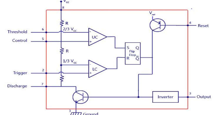
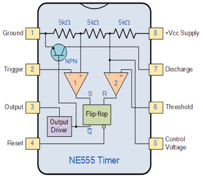
Pin Configuration of IC 555
| Pins | Description |
|---|---|
| Pin1 | Ground: The ground pin connects the 555 timers to the negative (0v) supply rail |
| Pin 2 | Trigger: The negative input to comparator No 1. A negative pulse on this pin “sets” the internal Flip-flop when the voltage drops below 1/3Vcc causing the output to switch from a “LOW” to a “HIGH” state. |
| Pin 3 | Output: The output pin can drive any TTL circuit and is capable of sourcing or sinking up to 200mA of current at an output voltage equal to approximately Vcc – 1.5V so small speakers, LEDs, or motors can be connected directly to the output. |
| Pin 4 | Reset: This pin is used to “reset” the internal Flip-flop controlling the state of the output, pin 3. This is an active-low input and is generally connected to a logic “1” level when not used to prevent any unwanted resetting of the output. |
| Pin 5 | Control Voltage: This pin controls the timing of the 555 by overriding the 2/3Vcc level of the voltage divider network. By applying a voltage to this pin the width of the output signal can be varied independently of the RC timing network. When not used it is connected to the ground via a 10nF capacitor to eliminate any noise. |
| Pin 6 | Threshold: The positive input to comparator No 2. This pin is used to reset the Flip-flop when the voltage applied to it exceeds 2/3Vcc causing the output to switch from “HIGH” to “LOW” state. This pin connects directly to the RC timing circuit. |
| Pin 7 | Discharge: The discharge pin is connected directly to the Collector of an internal NPN transistor which is used to “discharge” the timing capacitor to the ground when the output at pin 3 switches “LOW”. |
| Pin 8 | Supply +Vcc: This is the power supply pin and for general purpose TTL, 555 timers are between 4.5V and 15V. |
Application of IC 555
- This IC is used to build a different electronic circuit like flashing LED, Police siren, music box, LED dice, metal detector, traffic lights, etc.