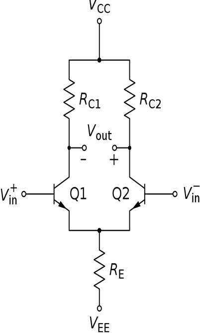
- The differential pair, also known as the long-tailed pair, is a common building block in electronic circuits, particularly in operational amplifiers. The topology predates the solid-state era and is widely credited to Alan Blumlein, who included it in one of his patents in 1936. Its usefulness stems from its ability to amplify the difference between two input signals while rejecting the portion of the signal that is shared by both inputs.
- Originally, this circuit was built with a pair of vacuum tubes. The circuit is the same for all three-terminal current gain devices. The bias points of a “long-tail” resistor circuit are largely determined by Ohm’s law, with active-component characteristics playing a smaller role.
- Differential amplifiers provide numerous benefits for manipulating differential signals. They offer immunity to external noise, a 6-dB increase in dynamic range (a significant benefit for low-voltage systems), and reduced second-order harmonics. Fully differential integrated amplifiers are ideal for driving differential ADC inputs and differential transmission lines.

- They make antialias filtering simple, and a dedicated input makes it simple to set the required common-mode voltage. These amplifiers are also suitable for driving differential transmission lines, and active termination improves efficiency. By implementing two symmetric feedback paths, you can easily convert inverting-amplifier topologies to fully differential amplifiers.
Working Principle of Long Tailed Pair
- The traditional differential pair amplifier is made up of at least two identical transistors, with the emitters of BJT transistors or the sources of FET transistors connected. A long-tailed pair (LTP), also known as an emitter coupled (source coupled) pair, is a pair of transistors in which the shared emitter or source node is supplied from a more or less constant current source/sink, which could be as simple as a relatively large value resistor connected to the negative supply, such as Rtail (or the positive supply for p-type devices), that develops a large voltage drop relative to the input signal, thus the “long tail.”
- The sum of the two collector or drain currents is also more or less constant with the signal given the more or less constant current supplied to the emitters or sources.
- The two inputs at the bases or gates can be fed a differential or balanced input signal, and the two outputs from the collectors or drains remain balanced; alternatively, one input can be grounded to convert a single-ended input signal to a differential output.
- The lower the common mode gain or Ac and the higher the common mode rejection ratio, the higher the resistance of the current source Rtail (CMRR). In more advanced designs, an active constant current source may be used in place of the high-resistance Rtail. This is a differential amplifier stage with two inputs and two outputs. The pair’s inputs are two bases or gates that are differentially amplified.
- Although this circuit is designed with two inputs and two outputs, both inputs and outputs are not required. (Recall that a differential amplifier has two possible inputs and two possible outputs.) A differential amplifier can be connected as a single-input, single-output, or differential-input, differential-output device. Depending on the needs of the subsequent circuitry, the output can be single-ended (taken from only one of the collectors or drains) or differential.
- In a long-tailed pair constructed with BJTs, the emitters are connected and then to the ground or a negative supply via the current source (for an LTP using NPN transistors). In this configuration, one of the transistors can be thought of as an amplifier with a common emitter, and the other as an emitter follower, feeding the other input signal into the first stage’s emitter, as discussed in the previous section. Because a transistor amplifies the current flowing between its base and emitter, the current flowing in the first transistor’s collector circuit is proportional to the difference between the two inputs.
- The bias condition assumes equal voltages at Vpos and Vneg, causing the bias current Itail (determined by Rtail) to be distributed equally between the transistors, resulting in IC1 = IC2. Equal voltages develop at Vout+ and Vout- when RC1 = RC2.
- We can build a source-coupled differential pair with MOSFETs, which is similar to the emitter-coupled differential pair with BJTs. When compared to BJTs, the main advantage of using MOSFETs for a differential pair is the nearly infinite input impedance, while the disadvantage is generally lower differential gain.
- Assuming the two MOSFETs are identical. For both common-mode and differential input signals, the source-coupled differential pair is analyzed in the same way as the emitter-coupled differential pair. The figure depicts the transfer characteristics of drain currents Id1 and Id2.
Differential Gain
- The differential voltage gain can be calculated as follows. Consider Q1 and Q2 as current sources whose base voltages are controlled. The currents are then converted back into voltages by RC1 and RC2. First, consider the low signal collector current.
![]()
- Where the DC collector current determines the transconductance gm (Amps/Volts).
![]()
- at standard room temperature RC then converts Ic back to voltage.
![]()
- When the input Vdiff = Vpos – Vnegin is added to the picture, it divides equally across the two base-emitter junctions, but with opposite polarities. When everything is put together, you get a single-ended output at each collector.
![]()
![]()
- When you subtract the two outputs, you get a differential output of
![]()
- As an example of how to set the bias: The bias is set by Rtail at Ie = (-0.6V – VDD) / Rtail = (-0.6V – (-15 V)) / 7.2 k = 2 mA, which divides equally between Q1 and Q2.
![]()
- Finally, gm = 1 mA / 25 mV = 0.04 A/V is a simple calculation. The single-ended gain is now.
![]()
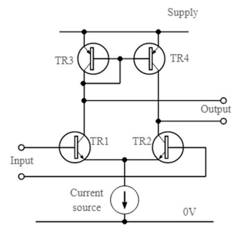
- A differential amplifier’s output is frequently differential. If this is not desired, only one output can be used, with the other output being ignored. Alternatively, a differential to the single-ended stage can be used after the differential stage to avoid sacrificing gain. Instead of collector/drain resistors, this is frequently implemented with an active current mirror load.
- Long-tailed pairs are commonly used in circuits that implement feedback linear amplifiers, such as operational amplifiers, and in other circuits that require a differential amplifier.
- When used as a switch, the “left” base or gate serves as the signal input and the “right” base or gate serves as the ground; output is obtained from the right collector or drain. When the input is zero or negative, the output is close to zero; when the input is positive, the output is most-positive; dynamic operation is the same as described above for the amplifier.
- Negative feedback introduced via emitter or source degeneration resistors can improve bias stability and independence from variations in device parameters.
Long Tailed Pair Collector Current Mirror
- Another enhancement to the basic circuit is the use of a current mirror within the transistor collector circuit. This allows the differential collector current signal to be converted to a single ended voltage signal without incurring resistor losses while increasing circuit gain.

- The current mirror’s high effective collector load enables voltage gains of 5000 or more to be achieved when no external load is applied to the circuit.
- The long tailed pair, also known as a differential pair, is widely used in integrated circuit technology, particularly in operational amplifiers, where it serves as the basic building block for the entire amplifier. Long tailed pair circuits made from discrete components are uncommon due to the ease of use and low cost of operational amplifiers. This demonstrates the op amp’s success and use of the long tailed pair circuit concept.
