CMOS Low Power Monostable/Astable Multi-Vibrator
- IC 4047 is a CMOS Low Power monostable/astable multivibrator mainly used for converting DC signal to AC signal. This inverter proves to be very handy in some countries where load-shedding creates a significant problem as it comes with the ability to store electrical energy and discharge it in the absence of main electrical power.
- For instance, 4047 IC has two independent monostable multivibrators that can be used as bistable
multivibrators. - The reason behind the use of two different monostable multivibrators is to enhance the efficiency and quality of the device.
- It is also vital to note that 4047 can generate sine waves between zero and 50Hz.
- It has a wide range of input voltage (3v to 18v) and DC input is up to ±10mA with a high operating temperature range of −55°C to +125°C.

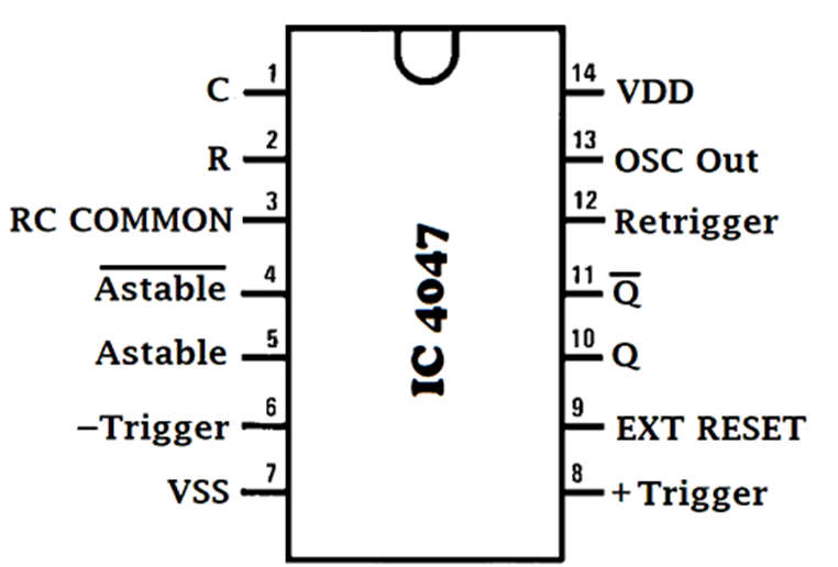
Pin Configuration

| Pin No. | Pin Name | Description |
|---|---|---|
| Pin 1 | C | Used to connect external capacitor |
| Pin 2 | R | Used to connect an external resistor |
| Pin 3 | RCC | Common pin for connecting resistor and capacitor to it |
| Pin 4 | AST | (Astable Low when used in Astable mode bar ) |
| Pin 5 | AST | High when used in Astable mode |
| Pin 6 | Trigger | Trigger |
| Pin 7 | Vss | Ground pin of IC |
| Pin 8 | + Trigger | When used in Monostable mode we give Low to High transition to this pin |
| Pin 9 | EXT RESET | It’s an external reset pin. By giving a high pulse to this pin resets the output Q to low and Q’ to high |
| Pin 10 | Q | Give the normal high output |
| Pin 11 | Q | Inverse output of pin 10, means it gives low output |
| Pin 11 | OSC | Out Gives oscillated output |
| Pin 14 | Vdd | Positive input pin of IC |
Specifications Of The 4047 IC
- For any single input, the DC input current is ±10mA.
- Has an operating range of temperature ranges from -55°C to +125°C.
- A 4047 IC chip has an input supply range of 3V to 18V.
- The storage temperature range of the 4047 IC is -65°C to +150°C.
- Its soldering lead temperature is 260°C.
Features Of The 4047 IC
- The buffered outputs are accurate and complimented.
- It has consistent and symmetrical o/p characteristics.
- Its inputs are consequently buffered.
- It is tested 100% for quiescent current on 20V.
- Can operate in monostable and astable modes.
- A single capacitor and resistor are required externally.
- The 4047 IC has less power utilization.
- In general, it has high noise immunity.
- The parametric ratings are 5 Volts, 10 Volts, and 15 Volts.
How to use 4047 IC?
- Multivibrators are devices that change the state of electrical signals on either a regular basis or according to the requirement. CD4047 is also a multivibrator IC. It can operate in two modes. A capacitor is connected externally between pins 1 and 3 to determine the pulse width of the output signal in the monostable mode and the output frequency is determined in astable mode by connecting a resistor between pins 2 and 3. A reset input is provided to reset the output of Q to 0 and the other output will become 1.
Monostable Mode of Operation
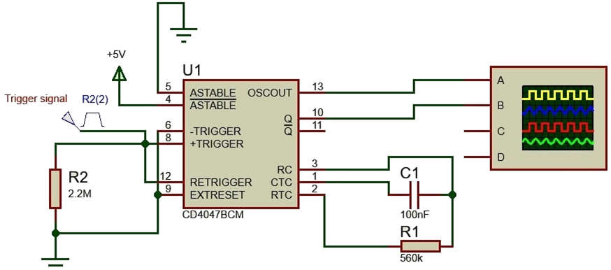
- The two inputs +trigger and -trigger are used to enable the monostable mode of operation. On applying +trigger input pin with low to high transition pulse and -trigger with high to low transition, the monostable output is obtained. The frequency of the outputs Q and ~Q can be calculated by the following formula.
f = 1/(8.8xRxC)
- The retrigger input is used to retrigger the device by trigging this input and +trigger input with low to high transition.
- To select, the monostable mode, connect the Astable pin with the ground and the astable pin with 5 volts.
- The diagram shown below indicates the behavior of CD4042 IC in monostable mode.
- In CD4047 monostable mode, we get output in the PWM form on the osc_out pin. Q output pin remains active high and ~Q active low.

Astable Mode of Operation
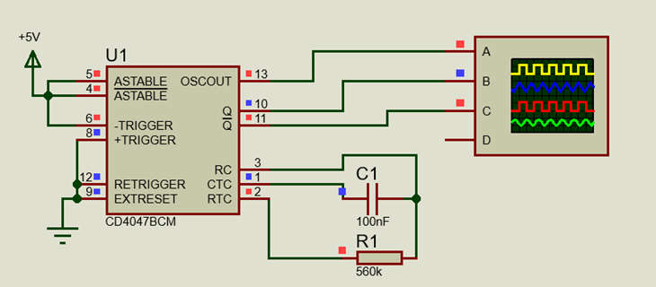
- The astable and ~astable inputs of CD4047 enable this mode of operation. The astable input connects with a high level. we can do it by applying a low level on input ~astable, the IC operates in an astable mode. The output frequency can be calculated through timing components and is given by the following equation.
f= 1/ 4.4xRxC
- In astable mode, we have an additional oscillator output. The timing diagram of the three outputs is shown below.

- The oscillator output at pin 13 is of the *basic frequency. The Q output frequency is half that of the basic frequency. Pin 11 output is the same as that of pin 10. But the output signal is inverted to 180 degrees. The time required to generate pulses is given by the formula.
t = 2.48×R×C
Applications of 4047 IC
- Convert DC to AC: This is the most common use of the 4047 IC. After all, most electronic devices and appliances use AC signals, making the conversion crucial.
- Convert AC to DC: This is another application of the 4047 IC. The IC can be used to convert AC to DC and vice versa.
- Convert audio signals: The 4047 IC is also commonly used as an audio signal converter. It can convert various audio signals into a form that is easily processed by other components such as transformers, amplifiers, etc.
- Multiplication of the frequency: This process entails taking the output of the 4047 IC and feeding it to another IC that is used to multiply the frequency.
- Generation of sine signals: This process entails taking the output of the 4047 IC, feeding it to another IC, and then feeding this output back to the first IC.
- Time delay applications: Time delay process entails taking the output of the 4047 IC and feeding it to another IC that is used to delay the signal.
- Frequency discriminators: Discrimination is a process whereby different frequencies and their amplitudes are selected. 4047 ICs are used in applications that require accurate frequency discrimination.
