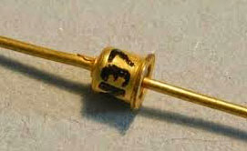
The tunnel diode was first introduced by Dr. Leo Easki in 1958. The Tunnel diode is high conductivity two terminal PN junction diode. It is heavily doped PN junction diode in which voltage increases and the electric current decreases.

The tunnel diode doping density is about 1000 times higher as compared to an ordinary junction diode. It is a low power diode. It reduces the width of the depletion layer to an extremely small value due to its heavy doping which reduces the reverse breakdown voltage to a very small. In the VI characteristic of the diode it produces a negative resistance region. It is called a tunnel diode because due to its extremely thin depletion layer, electrons are able to tunnel though the potential barrier at relatively low forward bias voltage which is less than 0.05V. Such diodes are manufactured from gallium arsenide (GaAs), germanium (Ge), and gallium antimonide (GaSb).
