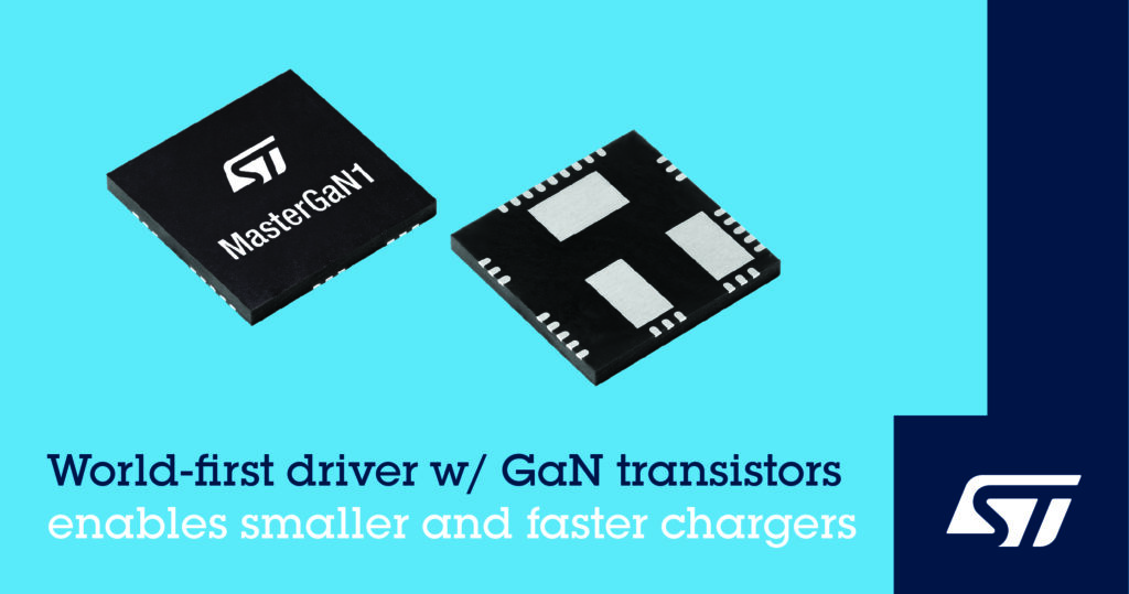
- World’s first solution to integrate Si driver and GaN power transistors in one package
- Enables chargers and adapters 80% smaller and 70% lighter, while charging 3 times faster compared to ordinary silicon-based solutions
October 13, 2020 – STMicroelectronics (NYSE: STM), a global semiconductor leader serving customers across the spectrum of electronics applications, has unveiled MasterGaN®, the world-first platform embedding a half-bridge driver based on silicon technology along with a pair of gallium-nitride (GaN) transistors. The combination will accelerate the creation of next-generation compact and efficient chargers and power adapters for consumer and industrial applications up to 400W.
GaN technology enables these devices to handle more power even as they become smaller, more lightweight, and more energy efficient. These improvements will make a difference for smartphone ultra-fast chargers and wireless chargers, USB-PD compact adapters for PCs and gaming, as well as in industrial applications like solar-energy storage systems, uninterruptible power supplies, or high-end OLED TVs and server cloud.
Today’s GaN market is typically served by discrete power transistors and driver ICs that require designers to learn how to make them work together for best performance. ST’s MasterGaN approach bypasses that challenge, resulting in faster time to market and assured performance, together with a smaller footprint, simplified assembly, and increased reliability with fewer components. With GaN technology and the advantages of ST’s integrated products, chargers and adapters can cut 80% of the size and 70% of the weight of ordinary silicon-based solutions.
“ST’s market-unique MasterGaN platform builds on our proven expertise and power-design skills to combine high-voltage smart-power BCD process with GaN technology, to accelerate the creation of space-saving and power-efficient products that are kinder to the environment,”said Matteo Lo Presti, Executive VP and General Manager Analog Sub-Group, STMicroelectronics.
ST is launching the new platform with MasterGaN1, which contains two GaN power transistors connected as a half bridge with integrated high-side and low-side drivers.
MasterGaN1 is in production now, in a 9mm x 9mm GQFN package only 1mm high. Priced at $7 for orders of 1,000 units, it is available from distributors.
An evaluation board is also available to help jump-start customers’ power projects.
Further technical information:
The MasterGaN platform leverages STDRIVE 600V gate drivers and GaN High-Electron-Mobility Transistors (HEMT). The 9mm x 9mm low-profile GQFN package ensures high power density and is designed for high-voltage applications with over 2mm creepage distance between high-voltage and low-voltage pads.
The family of devices will span different GaN-transistor sizes (RDS(ON)) and will be offered as pin-compatible half-bridge products that let engineers scale successful designs with minimal hardware changes. Leveraging the low turn-on losses and absence of body-diode recovery that characterize GaN transistors, the products offer superior efficiency and overall performance enhancement in high-end, high-efficiency topologies such as flyback or forward with active clamp, resonant, bridgeless totem pole PFC (power factor corrector) and other soft- and hard-switching topologies used in AC/DC and DC/DC converters and DC/AC inverters.
The MasterGaN1 contains two normally-off transistors that feature closely matched timing parameters, 10A maximum current rating, and 150mΩ on-resistance (RDS(ON)). The logic inputs are compatible with signals from 3.3V to 15V. Comprehensive protection features are also built in, including low-side and high-side UVLO protection, interlocking, a dedicated shutdown pin, and over-temperature protection.
For more information please go to www.st.com/mastergan1-pr
You can also read our blogpost at https://blog.st.com/mastergan1/
