- The material which can conduct the electricity within them are called conductors, and the material whose conductivity increases as soon as the light falls on it, that material is called a photoconductor.
- The increased electrical conductivity due to absorption of any type of light like infrared light, visible light, gamma rays, or ultraviolet light by the conductor material is called photoconductivity.
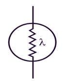
- The photoconductivity is mainly observed in semiconductors. And the symbol of the photoconductive cell is shown below.

- When a load resistor and bias voltage are used in series with a semiconductor, it is possible to monitor the voltage drop across the load resistor as the current in the circuit changes due to variations in the material’s electrical conductivity.
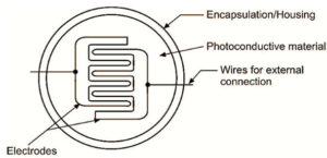
- Below is a diagram of the photoconductor’s creation. The base of the photoconductor is shaped like a disc, and a long strip of light-sensitive material is laid across it in a zigzag pattern. On each side of the strip, the connecting terminals are fastened to the conducting substance. To safeguard the light-sensitive material, a clear plastic cover is placed over a large strip of it that is located between the two conductors.

- To create photoconductive cells, two materials called CdSe (cadmium selenide) and CdS (cadmium sulfide) are used. These two materials react to variations in light intensity very slowly. Therefore, the response time for CdSe is about 10 ms, whereas the response time for CDS may be 100 ms.
- A fundamental internal semiconductor structure must be taken into account to fully comprehend this mechanism. When compared to conductors, the number of charge carriers like electrons in the conduction band is substantially lower in the energy-band diagram of semiconductors. But the valence band also contains charge carriers, such as holes.
![]()
- There are two types of semiconductors intrinsic and extrinsic. The pure semiconductor is called an intrinsic semiconductor and when impurities are added to it to increase its conductivity then it is called an extrinsic semiconductor.
- Multiple mechanisms by which photons cause electrons to be expelled from the valence band and injected into the conduction band result in the photoconductive effect. Intrinsic photoconductivity is the phenomenon in which the quantity of conduction electrons and holes rises simultaneously. P-type extrinsic photoconductivity is the phenomenon whereby more holes are created when electrons from a filled band are injected into empty impurity levels. The phenomenon is referred to as n-type extrinsic photoconductivity if electrons are expelled from impurity levels and injected into the conduction band. It is also feasible to excite intrinsic and extrinsic photoconductivity simultaneously.
Applications of Photoconductor
- Photoconductive materials are used in the manufacture of photoelectric devices.
- A simple application of photoconductive cells is for relay control. When the light on the photoconductive cell exceeds a particular value, the current through the circuit increases and the relay operates. When light is less, the current is not sufficient enough to energize the relay. The circuit for it is shown below.
![]()
- Making street lights turn on and off automatically according to the level of daylight.
