• Home
  • About Us
  • Contact Us
Semiconductor for You
"
  • Home
  • Semiconductor News
  • Technology
    • Automotive
    • Consumer Electronics
    • IoT
    • Lighting
    • Power Management
    • Wireless
    • Personal Electronics
    • Hardware & Software
    • Research
    • Medical Electronics
    • Embedded Design
    • Aerospace & Defence
    • Artificial Intelligence
  • DIY Projects
  • Market
  • Industries
    • Renesas Electronics
  • Knowledge Base
  • Events
  • Tools
    • Resistor Color Code Calculator
No Result
View All Result
Semiconductor for You
No Result
View All Result
Home Articles

P channel junction field effect transistor (JFET)

Semiconductor For You by Semiconductor For You
May 27, 2021
in Articles
0
ADVERTISEMENT

Construction:

P channel JFET
P channel JFET
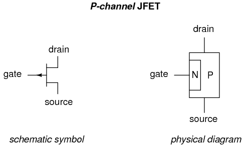
  • The construction of P channel JFET is similar to the N channel JFET excepts that it consist of a P type silicon bar with two N type heavily doped regions diffused on opposites sides of its middle part.
  • The JFET in which the current conduction takes place only due to holes as majority charge carriers is known as P channel JFET.
  • The two PN junctions are form by the N region and the space between i.e. P regions is called a channel. A single wire is taken in the form of the terminal when both the N type regions are connected internally known as the gate (G).
  • The electrical connection which is also known as ohmic contact are made to both ends of the P type semiconductor and are taken out in the form of two terminals called drain (D) and source (S).
  • The drain (D) is a terminal through which electrons enter the semiconductor bar and from through which the electrons leave the semiconductor is source (S) terminal.
Content Protection by DMCA.com
Tags: Semiconductorstransistor
Semiconductor For You

Semiconductor For You

Browse by Category

  • Aerospace and Defence
  • Articles
  • Automotive
  • Consumer-Electronics
  • Hardware & Software
  • Interview
  • IoT
  • Knowledge Base
  • Lighting
  • Market
  • personal-electronics
  • Power Management
  • Research
  • Semiconductor Events
  • Semiconductor News
  • Technology
  • Wireless
Semiconductor for You

Semiconductor For You is a resource hub for electronics engineers and industrialist. With its blend of
technology features, news and new product information, Semiconductor For You keeps designers and
managers up to date with the fastest moving industry in the world.

Follow Us

Browse by Category

  • Aerospace and Defence
  • Articles
  • Automotive
  • Consumer-Electronics
  • Hardware & Software
  • Interview
  • IoT
  • Knowledge Base
  • Lighting
  • Market
  • personal-electronics
  • Power Management
  • Research
  • Semiconductor Events
  • Semiconductor News
  • Technology
  • Wireless

Recent News

Infineon 2021 fiscal year off to a good start

Infineon, Visteon Collaborate to Deliver High-Performance Power Conversion for Next-Gen EVs

May 9, 2025
Infineon SEMPER™ NOR Flash memory family achieves ASIL-D functional safety certification

Infineon SEMPER™ NOR Flash memory family achieves ASIL-D functional safety certification

May 9, 2025
  • About
  • Advertise
  • Privacy & Policy
  • Contact

© 2022 Semiconductor For You

No Result
View All Result
  • Home
  • Semiconductor News
  • Technology
    • IoT
    • Wireless
    • Power Management
    • Automotive
    • Hardware & Software
  • Market
  • Knowledge Base
  • Tools
    • Resistor Color Code Calculator

© 2022 Semiconductor For You