By Catherine De Keukeleire, Director of Reliability & Quality Assurance, Wide Bandgap, onsemi
For decades, silicon (Si) has been the primary material for the semiconductor industry – used in everything from microprocessors to discrete power devices. However, with modern power demanding applications in areas such as automotive and renewable energy, the limitations of silicon are becoming more apparent.
As the industry looks for solutions, wide bandgap (WBG) materials including silicon carbide (SiC) and gallium nitride (GaN) are being seen as a solution. Bandgap describes the energy difference between the top of the valence band and the bottom of the conduction band. Silicon has a fairly narrow bandgap of 1.1 electronvolts (eV) while SiC and GaN have 3.3eV and 3.4eV respectively.
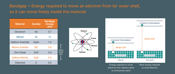
These characteristics mean that WBG materials behave more like insulators, and are able to operate at higher voltages, frequencies and temperatures. As a result, they are suited to power conversion applications such as electric vehicles (EVs) and renewable energy.
Silicon Carbide (SiC)
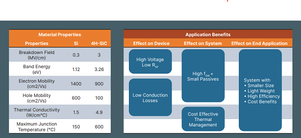
SiC is not new and has been manufactured for more than a century as an abrasive material. However, SiC is gaining prominence due to its attractive characteristics that make it suited to high voltage, high power applications. Physical properties such as high thermal conductivity, high saturation electron drift velocity, and a high breakdown electric field give SiC designs extremely low losses, faster switching speeds, and smaller geometries than silicon MOSFETs or IGBTs.
Many in the industry see SiC as a source of competitive advantage as it enables them to enhance efficiency while reducing size, weight and cost. As SiC systems operate at higher frequencies, passive devices are smaller and as losses are lower, less thermal mitigation is needed. Ultimately, this delivers the desired higher power densities that many modern applications demand.
Alongside the choice of material, implementing new die attach technologies in SiC power devices helps remove heat from devices. Techniques like sintering create a solid bond between the die and the substrate and ensure reliable interconnectivity. Therefore, it can enhance heat transfer efficiency and improve thermal performance.
SiC is generally used in high voltage applications (>650V) although it comes into its own at 1200V and higher, becoming the best solution for solar inverters and EV charging. It is also a key enabler of solid-state transformers where semiconductors will replace magnetics.
Manufacturing Challenges
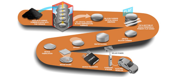
SiC is not easy to manufacture as, firstly, the granulate must be extremely pure and SiC boules require high levels of consistency. As SiC material can never be liquid, crystals cannot grow from a melt and therefore require carefully controlled pressure in a vapor phase technique known as sublimation. To do this, SiC powder is placed in a furnace and heated beyond 2200 °C, subliming and crystallizing on a seed. Even so, growth rates are slow – up to 0.5 mm per hour.
The extreme hardness of SiC makes it hard to cut, even with a diamond saw, which makes the creation of wafers more challenging than with silicon. While other techniques can be used, they can introduce defects into the crystals.
As SiC is a highly defective material and doping is challenging, producing larger wafers with few defects is not easy. Nevertheless, companies such as onsemi are now routinely producing 8-inch substrates.
Supporting Research
onsemi recognizes the importance of academia in developing semiconductor technology. In the case of SiC, research is under way in areas such as:
- Ruggedness regarding cosmic rays
- Intrinsic lifetime modeling for gate oxide
- SiC/SiO2 interface characterization and lifetime modeling
- Extrinsic population (screening)
- Epitaxy and substrate defectivity
- Body diode degradation
- High voltage blocking reliability (HTRB)
- Specific performance metrics regarding edge termination, avalanche robustness, and short circuit
- Design for high dv/dt ruggedness
- Surge currents.
Furthermore, onsemi has committed USD8M to a strategic collaboration around the onsemi Silicon Carbide Crystal Center (SiC3) at Pennsylvania State University (PSU). They are also working with at least six other educational establishments in Europe to further the technology.
The onsemi Manufacturing Advantage
onsemi is unique in that the company offers a fully integrated supply chain for SiC devices, allowing full control of all aspects of the process and associated quality – right from the boule to the customer.
The process starts in New Hampshire by growing single crystal SiC material, to which a thin epi layer is then added. Next, several device processing steps and packaging are completed to produce the final product.
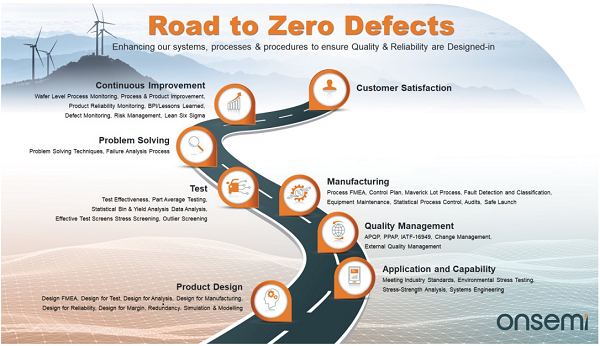
The end-to-end capability within onsemi production sites facilitates the fullest possible testing and supports root cause analysis. The goal is highly reliable products with zero defects.
With visibility into and control over every step, capacity can be scaled relatively easily to meet growing demand. Additionally, the process can be honed to maximize yield and control costs. Indeed, McKinsey & Company acknowledged the benefit of a vertically integrated supply chain when they wrote “vertical integration in SiC wafer and device manufacturing can improve yield by five to ten percentage points.”
Five Steps to Success
When addressing SiC-specific challenges, onsemi adopts a five-step methodology to address issues such as substrate and epitaxy defect levels, body diode degradation, reliability during high-voltage blocking and application related performance.
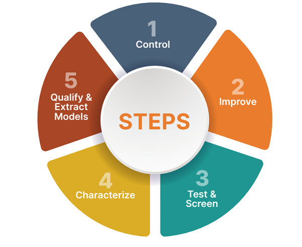
Gate Oxide Integrity (GOI) is crucial and is an area where the five-step approach is used.
Control – Tools such as a control plan, statistical process control and process failure mode and effects analysis (FMEA) are deployed, data is collected and used for process improvement.
Improve – Defects in the substrate or epitaxial layer as well as metallic contaminants and particles can all affect GOI. Continuous improvement lessens the occurrence of such defects.
Test & Screen – Visual and electrical screening are both used to identify any defective dies. Substrates are scanned and scanning continues during wafer processing, understanding defects at each stage. Electrical testing is performed at wafer level including burn-in and wafer sort.
Characterize – Charge to failure (QBD) is used to measure GOI quality as it detects finer details. The testing has shown SiC to be 50x better than silicon for intrinsic QBD performance. Sample QBD testing is performed in production and wafers rejected if not meeting a pre-defined acceptance criterion.
Qualify & Extract Models – The intrinsic performance of the gate oxide is assessed via time-dependent dielectric breakdown (TDDB) stressing. Gate bias and temperature are combined to stress the SiC MOSFETs, and times−to−failures are recorded. Weibull statistical distributions are then used to extract the lifetimes.
The onsemi SiC Difference
onsemi understands the critical role of SiC in the future of power electronics – especially power conversion applications in areas such as automotive and renewable energy. This understanding is driving investment in manufacturing capacity and product innovations to ensure SiC reaches its full potential as soon as possible.
As a vertically integrated supplier, the whole process is under our roof and in our control – something no one else can claim. This controls cost and ensures a defect-free product delivered to automotive and industrial manufacturers.
