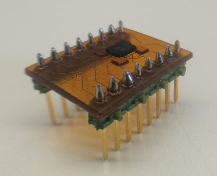
NESS ZIONA, Israel, April 24, 2019 –Nano Dimension Ltd., a leading additive electronics provider (NASDAQ, TASE: NNDM), announced today that the company’s pioneering DragonFly Pro systems have successfully shortened and simplified the assembly process for ball grid arrays (BGAs) and other surface mount technology (SMT) components used for integrated circuits, from days to one hour. This could not be achieved otherwise, due to the extended timelines and typically complex BGA assembly processes associated with traditional production methods.
In a recent qualification study, Nano Dimension’s Application Engineering team demonstrated the role of its award-winning DragonFly Pro, the only precision additive manufacturing system of its type worldwide, in enabling a shorter and simplified end-to-end process for mounting BGAs and other surface mounted electrical components into printed circuit boards (PCBs). Typically, the process from initial design through printing, soldering, manufacturing, assembly and reflow takes weeks to complete. With a special layout structure that can only be achieved through additive manufacturing of PCBs, there is no need for special tooling for assembly. This enables in-house manual assembly of BGAs and SMT components during the design and application development phase.
Electronic devices with BGA and other SMT components are found in everything from small devices such as phones and watches, to large vehicles and airplanes. BGAs are a type of surface-mount packaging (a chip carrier) used for integrated circuits. A BGA provides more interconnection pins than can be put on a dual in-line or flat package, since the entire bottom surface of the device can be used rather than just the perimeter.
The in-house approach enabled by the DragonFly Pro eliminates all the stages of ordering and delivering assembled PCBs from external suppliers and enables companies to do a lot more tests and feasibility studies that would not be possible without in-house additive manufacturing of electronics. Under existing practices, making needed design changes is tedious, as it involves back-and-forth communication between different suppliers, often leading to delays, creating difficulties in predicting development times, and putting the BGAs at a higher risk for errors. The DragonFly Pro 3D-printed socket structure even improves mounting accuracy of the BGA component since there is less risk that the mounting position will shift.
“With the DragonFly Pro, companies can easily assemble BGA components within one hour,” said Amit Dror, CEO of Nano Dimension. “This means companies can do everything in-house, with no need for outside contractors, less risk of errors and they can complete complex PCB prototypes without high volume manufacturing processes. Greater flexibility enables teams to innovate more freely, resolve problems quickly, and makes it much easier to control product quality.”
About Nano Dimension Ltd.
Nano Dimension (NASDAQ, TASE: NNDM) is a leading electronics provider that is disrupting, reshaping, and defining the future of how cognitive connected products are made. With its unique 3D printing technologies, Nano Dimension is targeting the growing demand for electronic devices that require increasingly sophisticated features. Demand for circuitry, including PCBs – which are the heart of every electronic device – covers a diverse range of industries, including consumer electronics, medical devices, defense, aerospace, automotive, IoT and telecom. These sectors can all benefit greatly from Nano Dimension’s products and services for rapid prototyping and short-run manufacturing. For more information, please visit www.nano-di.com.