Materials database
Electronic materials and nanocrystals are used in a variety of applications.
To integrate materials and crystals in devices, researchers must search in multiple places to discover new technologies and their various properties. On top of that, researchers may require long hours in the lab, and large computational resources, to enable new materials.
Seeking to help researchers, the Nordic Institute for Theoretical Physics (NORDITA) has developed a comprehensive database of organic and organometallic materials.
NORDITA’s so-called Organic Materials Database (OMDB) is a database that is freely accessible to researchers. It allows users to search for materials with specified target properties using advanced data mining techniques. The database involves the electronic structures, density of states and other properties for materials.
At present, the database consists of 6,686 calculated Kohn-Sham band structures. The structural information for the database was originally taken from the Crystallography Open Database (COD). The COD is an open-access collection of crystal structures of organic, inorganic, metal-organic compounds and minerals.
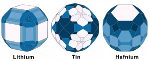
Others have launched similar research tools. For example, the University of California at San Diego and Lawrence Berkeley National Laboratory recently created an open-source database of elemental crystal surfaces and shapes. That database, called Crystalium, is a new and expanding set of information about various crystals. The database can help researchers design new materials for various applications, such as batteries, catalytic converters, fuel cells, semiconductors and others.
Here’s an example of Crystalium:

Faster material development
In a separate effort, Northwestern University and Los Alamos National Laboratory have developed a workflow to create design guidelines for new materials.
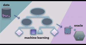
The workflow combines machine learning and density functional theory calculations. Using this technique, researchers focused on the development of a class of two-dimensional complex oxides, dubbed Ruddlesden-Popper oxides. These materials exhibit ferroelectricity and piezoelectricity.
To devise these materials, researchers built a database of known materials. More than 3,000 possible materials were investigated. Using machine learning, researchers narrow that down to more than 200 promising candidates.

Finally, they narrowed it down to 19 possibilities. “In this family, the data set is puny. Currently, there are only around 10 to 15 materials that are known with the desired properties,” said James Rondinelli, assistant professor of materials science and engineering in the McCormick School of Engineering at Northwestern. “This is not much data to work with. Traditionally data science is used for big data problems where there is less of a need for domain knowledge.”
Prasanna Balachandran of Los Alamos National Lab added: “With machine learning, we are able to identify chemical compositions that are likely candidates for the material you want to develop.”
Better TFETs
At one time, the tunnel field-effect transistor (TFET) was among the top candidates in the next-generation transistor race at 5nm and beyond.
TFETs are steep sub-threshold slope transistors that can scale the supply voltages below 1 volt, and possibly as low as sub-0.5 volts. The TFET is similar to today’s MOSFETs, but the TFET is a gated-diode that makes use of an electron tunneling technology. In theory, TFETs could switch on and off at lower voltages than current and future finFETs.
But putting TFETs into production is difficult. TFETs may require III-V materials, nanowires and other complex technologies. So far, the overall performance of TFETs is not better than today’s finFETs. All told, the excitement and progress for TFETs has subsided.
Seeking to jumpstart the development of the technology Imec has presented promising results with its latest efforts in TFETs. The device developed at Imec is based on a III-V technology called indium gallium arsenide (InGaAs). Basically, Imec’s TFET is an InGaAs-only or an InGaAs homojunction TFET.
The device shows a minimum sub-threshold swing of 54mV/dec at 100pA/mm. The sub-threshold swing remains sub-60mV/dec over 1.5 orders of magnitude of current at room temperature. The EOT of the devices is 0.8nm, which helps with the desired sub-60 mV/dec performance.
“We have entered an era where new chip technologies require making trade-offs between power, performance, cost and area. And these trade-offs will be considered separately for different application domains,” said Nadine Collaert, a distinguished member of the technical staff at Imec. “TFETs will most probably find their place in the ultralow-power segment. Many applications in the future require transistors to work at low power and low voltage, such as the many Internet of Things applications.”
