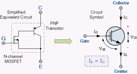
The IGBT stands from Insulated gate bipolar transistor. It is a three terminal semiconductor device is named as gate, emitter and collector.
The terminals of the IGBT are associated with a conductance path and gate terminal is associated with its control.

When the gate terminal is positive with respect to emitter and with gate- emitter voltage more than the threshold voltage of IGBT, an n-channel is formed in the p-regions as in a power MOSFET (metal oxide semiconductor field effect transistor).
This n-channel short circuits the n– region with n+ emitter regions. An electron movement in the n-channel, in turn causes substantial hole inject from p+ substrate layer into the epitaxial n– layer. Ultimately a forward current is established show in fig.
