What is a FET (Field Effect Transistor)?
- A Field Effect Transistor (FET) is a three-terminal Active semiconductor device in which an electric field produced by the input voltage regulates the output current. Because, unlike bipolar transistors, FETs only use either electrons or holes as charge carriers, they are also referred to as unipolar transistors.
- The Field Effect Transistor (FET) is a “Voltage” operated device because it uses the voltage applied to its input terminal (known as the Gate) to control the current flowing from the source to the drain.
- Due to their small size and significantly lower power consumption, FETs are widely used in Integrated Circuits (ICs). In addition, FETs are utilized in logic circuits, operational amplifiers (Op-Amps), tone controls, and high power switching applications as voltage-variable resistors (VCRs) and tone controls, respectively.
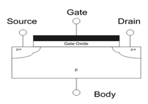
- The Source, Drain, Gate, and Body terminals on a FET are its four terminals.
- The terminal known as the Source is where the majority of charge carriers are introduced into FETs.
- The Drain terminal is where the majority of charge carriers leave the FET.
- The Gate terminal is created through the diffusion of an N-type and a P-type semiconductor. As a result, a region of the PN junction that is heavily doped regulates the carrier’s flow from source to drain.
- The substrate on which the FET is constructed is called the Body. Since it is internally connected to the source pin in discrete applications, its effects can be completely disregarded. However, because it will be shared by several transistors in integrated circuits, this pin will typically be connected to the most negative power supply in an NMOS circuit (or the most positive in a PMOS circuit). When the Body connection is involved, careful connections and design are essential to maintaining FET performance.
- The majority of carriers pass through the Channel as they travel from the source terminal to the drain terminal.
Classification of FET
Based on its construction FET’s are classified as
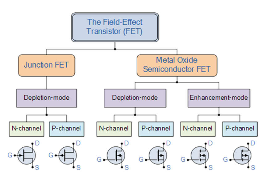
1. JFET (Junction Field Effect Transistor)
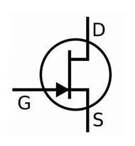
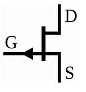
- The channels that form between the terminals are the foundation for how these JFETs function. Either the n-type or the p-type of the channel may exist. It is known as an n-channel JFET because of the n-type channel, and a p-channel JFET because of the formed p-type channel.
Working of FET
- JFET construction is similar to that of BJT in that it can be formed using n-type and p-type materials. The n-type is sandwiched between the p-types, or the p-types are sandwiched between the n-types. These, like N-P-N and P-N-P transistors in BJT, are also formed in FET. These JFETs have a channel that can be n or p-type.
- It is classified as an n-channel JFET or a p-channel JFET depending on the channel.
- The positive side of the n-channel JFET is connected to the source terminal.
- In this n-channel JFET, the drain terminal has the highest potential compared to the gate.
- The junction formed by the interaction of the drain and the gate terminal will be biased in the opposite direction.
- As a result, the width of the depletion region near the drain is greater than the width of the depletion region near the source.
- Because of this, the majority of the charge carriers, which are electrons, can be seen flowing from the terminal drain to the source.
- As the potential at the drain tends to increase the flow of carriers, so does the flow of current.
- However, when the voltages at the drain and source are increased, the current flow is stopped.
- The JFET is well-known for its ability to control current through the application of input voltages.
- In this transistor, the input impedance has reached a maximum.
- There is no current evidence at the gate terminal when the JFET is in its ideal mode.
- That is how an n-channel JFET operates. Only by varying the polarities of the supplies does the FET function as a p-channel JFET.
1. MOSFET(Metal Oxide Semiconductor Field Effect Transistor)
- The operation of MOSFETs is based on the channels that exist or form when a voltage is applied. MOSFETs are classified into two types based on their modes of operation: depletion mode and enhancement mode. In the enhancement mode, the channel is induced by applying a voltage to the gate, whereas in the depletion mode, the MOSFET operates due to the already existing channel.
- The N-channel MOSFETs are known as NMOS and are represented by the symbols shown below.
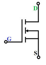
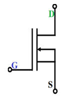
- PMOS is P-Channel MOSFETs, and they are represented by the symbols below.

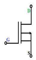
- A channel is formed in the enhancement mode when a voltage applied to the gate terminal exceeds a threshold voltage. It could be n-type for a P substrate and p-type for an N substrate. The enhancement mode is classified as N-type Enhancement MOSFET or P-type Enhancement MOSFET based on the channel formation. MOSFETs of the enhancement type are more commonly used than those of the depletion type.
Characteristics of FET
The characteristics of FETs are primarily determined by their operating regions. The four regions are ohmic, saturation, cut-off, and breakdown.
1. Ohmic Region
- The ohmic region is defined as the region where the transconductance exhibits a linear response and the current at the terminal gate is opposed by resistance.
2. Saturation Region
- The device is fully ON in this region. The maximum amount of current flows through the transistor at a steady state during this condition.
3. Cut-off Region
- During this region, there is no current flowing through the transistor. As a result, it is referred to as the device in the OFF state.
4. Breakdown Region
- When the applied voltage exceeds the maximum value of the voltage, the transistor enters the breakdown condition, indicating that it resists the flow of current.
Advantages of FET
- The input impedance of a FET is several megaohms.
- Radiation has less of an effect on FET than it does on BJT.
- Temperature stability greater than BJT.
- When compared to BJT, there is less noise.
- Can be manufactured with less processing and a smaller size.
- Longevity and efficiency.
- It is applicable. application with low frequency.
- Unipolar Device.
- Device for controlling voltage.
- They are more thermally stable.
- They have a voltage regulator.
Disadvantages of FET
- They cost more than junction transistors.
- When compared to BJT, this product has a lower gain bandwidth.
- Because the transconductance is low, the voltage gain is also low.
- It has a faster switching time than a BJT.
- During installation, special care must be taken.
- When the performance of a FET degrades as the frequency increases. This is due to feedback from internal capacitance.
Applications of FET
- FETs are widely used in integrated circuits because they take up less space than BJT chips.
- FETs are used as voltage-variable resistors (WRs) in operational amplifiers (op-amps), tone controls, FM and TV receiver mixers, and logic circuits.
- Despite their lower operating speed, FETs are commonly used in digital switching circuits.
Other applications of FET are
- Low Noise Amplifier
- Buffer Amplifier
- Cascode Amplifier
- Analog Switch
- Chopper
- Multiplexer
- Current Limiter
- Phase Shift Oscillators
