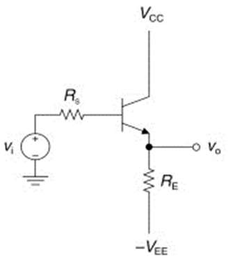
- Emitter follower is a more popular name for the ubiquitous collector circuit design. The emitter follower is a buffer stage with an approximately unity gain, high input impedance, and low output impedance.
- It is a circuit with negative current feedback. The emitter follower is a voltage-gainless current amplifier. The fact that it has a high input impedance and a low output impedance is its most crucial feature. It is the perfect circuit for impedance matching because of this.
- The emitter follower or common collector stage electronic circuit design is very simple, requiring only a few electronic components and some very simple calculations.

- The name “common collector transistor circuit configuration” comes from the fact that the collector circuit is shared by both the input and output circuits, with the base associated with only the input and the emitter with only the output.
- The common collector is also known as an emitter follower. The name comes from the fact that the emitter voltage “follows” the base voltage – the circuit has unit voltage gain.
Working of Emitter Follower
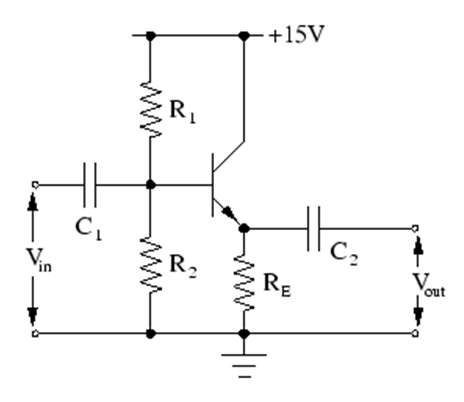
- Figure below depicts an emitter follower circuit. The absence of a collector load and an emitter bypass capacitor distinguishes it from the circuitry of a conventional CE amplifier. The emitter resistance RE serves as the load, and the alternating current output voltage (Vout) is measured across RE. Biasing is typically accomplished through the use of a voltage divider or a base resistor. The emitter follower should be noted for the following reasons.

- There is no collector resistor or emitter bypass capacitor in the circuit. These are the emitter follower’s two circuit recognition features.
- Because the collector is at the alternating current ground, this circuit is also known as a common collector (CC) amplifier.
- When an input voltage is applied between the base and the emitter, the resulting alternating current emitter current generates an output voltage ieRE across the emitter resistance. This voltage is in opposition to the input voltage, resulting in negative feedback. The voltage feedback is proportional to the emitter current, i.e., output current, indicating that it is a negative current feedback circuit. The output voltage follows the input voltage, hence the name emitter follower.
Characteristic of Emitter-Follower
The following are the main characteristics of an emitter follower.
- There is no voltage gain. The voltage gain is almost one.
- Current gain and power gain are both relatively high.
- Input impedance is high, and output impedance is low.
- The alternating current voltages at the input and output are in phase.
Designing an Emitter-Follower
- The purpose of an emitter follower circuit is to serve as a buffer. It simulates the effect of a buffer because it has a high input impedance and a low output impedance.
- As a result, if a voltage line needs to be buffered, it can be connected to the circuit’s input, and the load that needs to be powered connects to the circuit’s output.
- In our circuit, the input impedance will be greater than 50K and the output impedance will be around 5. This produces a reasonably effective buffer effect on any voltage that needs to be buffered.
- Several factors must be considered when designing an emitter follower circuit, including how much DC voltage is supplied to the transistor’s collector, how much current is desired to be passed through the transistor, and the frequency cutoff of the AC signals entering the input. All of these ideas will be discussed in detail further down.
Choose a Transistor:
- As previously stated, the transistor type should be chosen based on the expected performance requirements.
Select Emitter Resistor:
- Determine the current required from the impedance of the following stage using an emitter voltage of about half the supply voltage to give the evenest range before the onset of any clipping.
Determine Base Current:
- Determine the maximum base current by dividing the collector current by (or hfe which is essentially the same).
Determine the Base Voltage as Follows:
- The base voltage is simply the emitter voltage plus the base-emitter junction voltage, which for silicon transistors is 0.6 volts and for germanium transistors is 0.2 volts.
Calculate the Base Resistor Values:
- Assume a current flowing through the chain R1 + R2 that is approximately ten times the base current required. Then, choose the correct resistor ratio to provide the required voltage at the base.
Determine the Value of the Input Capacitor:
- To achieve a -3dB drop at the lowest frequency, the value of the input capacitor should equal the resistance of the input circuit. The total impedance of the circuit will be times R3 plus any external resistance, i.e. the source impedance. The external resistance is frequently ignored because it is unlikely to have a significant impact on the circuit.
Calculate the Output Capacitor Value:
- Again, the output capacitor is typically selected to equal the circuit resistance at the lowest operating frequency. The circuit resistance is the sum of the emitter follower output resistance and the load resistance, i.e. the circuit following.
Reassess Your Assumptions:
- Re-evaluate any circuit assumptions in light of how the circuit has evolved to ensure they are still valid. Aspects such as transistor selection, current consumption values, and so on.
Output Characteristics

Applications of Emitter Follower
- The emitter follower configuration’s applications revolve around its key features of unity (voltage) gain, current amplification, and impedance matching. In practice, they will be used inside many ICs, and you may not even realize you are using them. Some simple applications you can try at home take advantage of the fact that the output voltage in this configuration can be controlled from the transistor’s base:
- Amplifiers.
- Motor control.
- Adjustable power supplies.
- Adjustable Zener diodes.
