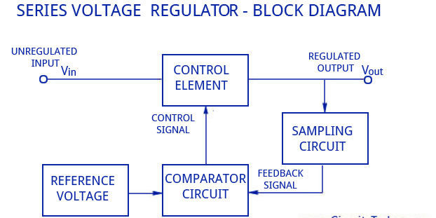
The block diagram of transistor series voltage regulator is shown in above figure. In the transistor series voltage regulator the control element is connected in series with the load, due to this circuit is known as series voltage regulator. When the control element is in series with the load, the output is given by
VOut = VIn – VS
The voltage drop across the control element is VS. The comparator circuit compares the feedback signal with a constant reference voltage and produces a control signal which is applied to the control element.
Depending on the value of control signal the voltage VS across the control element is adjusted in order to maintain the output voltage constant. For example if the output voltage increases above its regulated value then the feedback signal increases, the control element is increased to reduce the output voltage to its regulated value.
If the output voltage decreases then exactly the opposite action will take place to maintain the output the output voltage constant. The control element has to carry the load current because it is in series with the load. Therefore the control element must have high current rating as well as high power rating. Under normal operating conditions, voltage drop VS across the series control element is 2 V to 37 V.
Therefore Vin has to be greater than VOut by this amount. The series regulator exhibits a better performance as compared to a shunt regulator. It is preferred when variable output voltage is required. The function of a comparator in transistor series voltage is to compare the feedback signal with a constant reference voltage for producing a control signal which is applied to the control element. After combination it produces the error signal proportional to the changes in the output voltage.