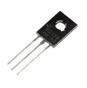
- BD139 is an NPN transistor hence the collector and emitter will be left open (Reverse biased) when the base pin is held at the ground and will be closed (Forward biased) when a signal is provided to the base pin.
- The gain value of BD139 ranges from 40 to 160, and this value determines the transistor’s amplification capacity. Because the maximum current that can flow through the Collector pin is 1.5A, we cannot connect loads that consume more than 1.5A to this transistor.
- To bias a transistor, we must supply current to the base pin; this current (IB) should be limited to one-tenth of the collector current, with a maximum voltage of 5V across the base-emitter pin.
- When fully biased, this transistor can allow a maximum of 1.5A to flow across the collector and emitter. This is known as the Saturation Region, and the typical voltage allowed across the Collector-Emitter (VCE) or Base-Emitter (VBE) is 80V. When the base current is removed, the transistor turns completely off; this is referred to as the Cut-off Region.

- We should now understand what an NPN transistor is and how it works, which will help us understand how and where we can use the 2N5551 transistor in practical applications.
- NPN transistors are those that have one p-type material sandwiched between two n-type materials. The NPN transistor amplifies the weak signal that enters the base and generates high-amplitude signals at the collector end.
- In an NPN transistor, an electron moves from the emitter to the collector region, causing current to flow through the transistor. This type of transistor is commonly used in circuits because its majority charge carriers are electrons, which have higher mobility than holes.
- A small voltage VBE is observed when the emitter-base junction is forward biased. VCE is the reverse bias voltage. The majority of charge carriers in the emitter are repelled towards the base due to the forward bias. Because the base is lightly doped, electron-hole recombination is very low in the base region. The majority of electrons enter the collector region.
- When the emitter is forward biased, electrons flow towards the base, producing the emitter current IE. The majority of the charge carriers in the P-type material combine with the holes here.
- Because the NPN transistor’s base is lightly doped, only a few electrons can combine, and the remaining current is known as the base current IB. When the collector region is skewed in the opposite direction, it exerts a greater force on electrons approaching the collector junction, attracting electrons at the collector.
Features and Specifications of BD139 NPN Transistor
- DC gain products are pre-selected.
- VCE (collector to emitter voltage) is 80V.
- The collector current (Ic) is 1.5 amps.
- Pd (power dissipation) is 12.5W.
- At 0.5A collector current, the collector to emitter saturation voltage is 500mV.
- The DC gain (hFE) is 25.
- The operating junction temperature range starts at 150°C.
Pin Configurations
- The pin diagram of the BD139 NPN transistor is shown below.
-
- Emitter – Current drains through the emitter, which is normally connected to ground.
- Collector – Current enters the collector, which is normally connected to the load.
- Base – Controls the biasing of the transistor; used to turn the transistor ON or OFF.
Applications of BD139 NPN Transistor
- Because of the high collector current of 1.5A, this transistor can control (on/off) high loads that consume less than 1.5A.
- The saturation voltages (Base Emitter Voltage VBE) of only 5V make it suitable for use in digital electronics with an operating voltage of 5V.
- It is used as RF Amplifiers.
- It is used in switching circuits.
- It is used in amplification circuits.
- It is used in audio amplifiers.
- It is also used in Load driver circuits.