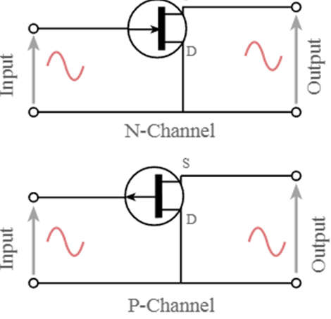
- A common-drain amplifier, also known as a source follower, is one of three basic single-stage field-effect transistor (FET) amplifier topologies used as a voltage buffer in electronics. The gate terminal of the transistor serves as the signal input in this circuit (NMOS), the source is the output, and the drain is common to both (input and output), hence the name. The common-collector amplifier is an analogous bipolar junction transistor circuit. This circuit is also known as a “stabilizer.”
- The drain terminal is connected to AC ground in the Common Drain Amplifier configuration. The input is connected to the gate and drain terminals, while the output is connected to the source and drain terminals.
- Because the drain terminal is shared by the input and output sides, it is referred to as a Common Drain Amplifier.

- When an input signal is applied to the gate, the input resistance seen by the input signal source is extremely high, just as it is in a common-source amplifier configuration. The total input resistance is the gate resistor, RG, in parallel with the input resistance looking in at the gate.
- The transistor emitter follower, source follower configuration provides a lot of buffering and a lot of input impedance. Because it is a field effect device, the FET’s actual input resistance is very high. This means that the source follower circuit can perform admirably as a buffer.
- Although the voltage gain is one, the current gain is high. The input and output signals are synchronized.
- Common-drain can transform a subpar voltage source into a nearly perfect one.
- The addition of bypass capacitors on the drain terminal of the FET, this was added to the resistance that only affects the circuit’s DC functionality. In AC operation, the drain terminal will be an AC ground, which corresponds to the circuit analysis.
- The output voltage is at the source and is in phase with the gate voltage (input).
FET Common Drain Circuit
- The typical implementation of the common drain or source follower / buffer circuit is extremely simple to implement in practice.
- The circuit depicted below is an example of a FET source follower / buffer circuit. C1 and C2 are capacitors that couple the AC signal between stages while blocking the DC elements. The gate bias is provided by resistor R1, which keeps the gate at ground potential. The resistor R2 is connected to ground in the source circuit, and its value is determined by the required channel current.
![]()
- The source follower circuit has a very high impedance to the preceding stage, making it an ideal format for use as a buffer.
Expression for Common Drain JFET Amplifier
- The equivalent circuit for the circuit discussed above is shown below.
![]()
- Since rd and RS are in parallel, so their equivalent resistance is given by,
![]()
- Output voltage Vo for common drain JFET amplifier is given by,
![]()
- Using eqn. (1), we get,
![]()
- The input signal applied between gate and drain is represented by the input voltage Vi which is given by,
![]()
- Now, voltage gain (Av) is given by,
![]()
- Since rd >> RS, so eqn. (3) can be written as,
![]()
