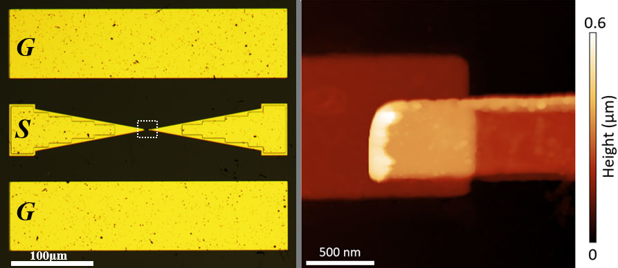
Two-dimensional, atom-thin materials are good for a lot of things, but until two years ago, nobody thought they’d make good memory devices. Then Deji Akinwande, Jack Lee, and their team at UT Austin tried it out. It turns out that sandwiching a 2D material like molybdenum disulfide between two electrodes makes a memristor—a two-terminal device that stores data as a change in resistance. In research reported last week, they’ve proved a very important potential application for these “atomristors”—analog RF switches for 5G and perhaps future 6G radios.
Cellular radios do a lot of switching. They have to switch between transmit and receive, they have to switch between different frequencies to prevent interference, and they may have to switch among signals with different phases to steer their data beams around. RF switches are pretty demanding devices that need a combination of characteristics that are hard to come by. Fast switching, low on resistance, high off-impedance, little leakage, and—this is the part today’s switches don’t do—they should stay in place without power. Battery-dependent IoT systems could potentially last longer if they didn’t have to keep radio switches powered up. That’s what the new nanoscale atomristor switches can now do, not just for 5G frequencies but for possible future 6G frequencies, as well.
Memristors are generally made up of two electrodes sandwiching a pillar of insulating material, such as an oxide material. The device starts off in a high-resistance state, preventing current from passing through it. But raise the voltage high enough, and oxygens are shoved out of place in the oxide to form a conductive pathway. In this state, the device now passes current easily. A high voltage in the reverse direction puts the oxygens back in place, restoring its resistance.

But that can’t be what’s happening in 2D semiconductors, because there’s no vertical dimension to form a conductive path. Instead, Akinwande’s group found, certain naturally occurring defects in the two-dimensional material’s crystal lattice produce the effect. These defects are missing atoms. Ordinarily, the resistance across the 2D material is high, but with enough voltage, gold atoms from the electrodes will temporarily move into the vacancies making the material conductive. “Basically, it’s like Airbnb. They’re just renting the space,” says Akinwande. A strong reverse voltage will push the gold back out.
The atomristor-action was initially discovered using molybdenum disulfide as the 2D material. But for RF switches, which have to strongly block signals when switched off, “what you really need is an insulator,” says Akinwande. So the team and their collaborators at University of Lille turned to hexagonal boron nitride (hBN), an extensively studied 2D insulator.
“Usually when people use hBN, they’re using several layers,” says Akinwande. But over time his team was able to build switches with just a single, 0.3-nanometer-thick layer of material. “People were shocked by this result.” The key was to produce hBN without any flaws big enough to let current leak through. “It has to be near perfect, but not perfect,” he says.
The key figure of merit for RF switches is called cut-off frequency. It’s a combination of on-state resistance and off-state capacitance, both of which should be low in a good switch. Terahertz values for cutoff frequency indicate that a device is a good candidate for an RF switch, and the experimental hBN devices scored 129 terahertz. As part of the testing, the team transmitted real-time high-definition video at a rate of 8.5 gigabits per second using a 100 gigahertz carrier frequency, which they say is more than sufficient for 5G’s streaming needs. At this data rate, several movies can be downloaded in a few seconds. They reported their results in Nature Electronics.
For 5G frequencies, Akinwande is exploring commercialization to further develop the nanometer-scale switches. Although the research device was demonstrated using gold electrodes on a diamond substrate, Akinwande says the process for making these RF switches is compatible with the CMOS processes used in foundries. He points to research done at several universities and TSMC showing the integration of hBN with silicon.
For 6G frequencies, which are expected to include frequencies in the terahertz range (300 to 3000 GHz), the UT Austin team is planning new laboratory measurements.
