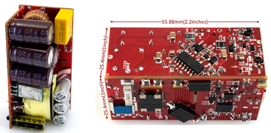
OTTAWA, Ontario, March 11, 2021 – GaN Systems, the global leader in GaN (gallium nitride) power semiconductors, announced today a new reference design for the highest power density, high efficiency GaN-based 65W Active Clamp Flyback (ACF) charger in collaboration with Silanna Semiconductor. The reference design is now available at Silanna Semiconductor and provides an easy design for ACF USB-C PD GaN chargers, reducing design cycles and product time to market for customers.

This solution removes the difficulties of an ACF topology design, which typically has two transistors in the high-side and in low-side configuration. The new charger reference design uses Silanna Semiconductor’s SZ1130 ACF Pulse Width Modulator (PWM) controller and GaN Systems GS-065-008-1-L 650V GaN power transistor, with the high-side FET integrated into the controller. This design results in lower BoM costs by using a conventional RM8 transformer and 100V SR MOSFET on the secondary side.
Key Benefits and Features:
- Ultra-high density: 30W/in^3 no case
- High efficiency: peak efficiency >94%
- Low temperature: <95◦C max component temperature
- Better EMI design: Clean waveforms with almost zero voltage spike or ringing
Supports wide range of applications: 5V/3A, 9V/3A, 15V/3A and 20V/3.25A output voltages; USB-PD
“Silanna Semiconductor’s SZ1130 chip is a great fit for 65W ACF designs and is another example of a company developing an innovative solution in recognition of the growing importance of GaN to power engineers,” says Jim Witham CEO of GaN Systems, “As GaN becomes the standard building block across markets, it’s good to see that the ecosystem continues to grow.”
For more information or to purchase, please visit www.gansystems.com or Silanna Semiconductor at www.powerdensity.com.
