Copying technique could cut the cost of compound semiconductor devices

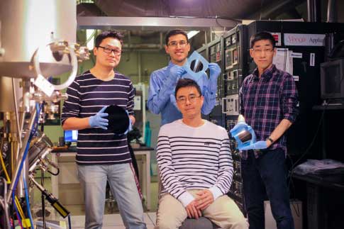
Left to right: Postdoc Kyusang Lee, Professor Jeehwan Kim (sitting), and graduate students Samuel Cruz and Yunjo Kim.
A new technique dubbed ‘remote epitaxy’ by MIT engineers could reduce the overall cost of semiconductor wafers and cut the cost of devices made from expensive compound semiconductor materials.
The method, reported in Nature, uses graphene to transfer intricate crystalline patterns from the underlying semiconductor wafer to a top layer of identical material.
The engineers worked out ways to place single sheets of graphene onto a wafer. They then grew semiconducting material over the graphene layer.
They found that graphene is thin enough to appear electrically invisible, allowing the top layer to see through the graphene to the underlying crystalline wafer, imprinting its patterns without being influenced by the grapheme.
The researchers successfully applied the technique to InP, GaAs and GaP – materials that are 50 to 100 times more expensive than silicon.
Graphene is ‘slippery’ and does not tend to stick to other materials easily, enabling the engineers to peel the top semiconducting layer from the wafer after its structures have been imprinted.
Jeehwan Kim, a professor in the departments of Mechanical Engineering and Materials Science and Engineering, says that in conventional semiconductor manufacturing, the wafer, once its crystalline pattern is transferred, is so strongly bonded to the semiconductor that it is almost impossible to separate without damaging both layers.
“You end up having to sacrifice the wafer – it becomes part of the device,” Kim says.
With the group’s new technique, Kim says manufacturers can now use graphene as an intemediate layer, allowing them to copy and paste the wafer, separate a copied film from the wafer, and reuse the wafer many times over. In addition to saving on the cost of wafers, Kim says this opens opportunities for exploring more exotic semiconductor materials.
“The industry has been stuck on silicon, and even though we’ve known about better performing semiconductors, we haven’t been able to use them, because of their cost,” Kim says. “This gives the industry freedom in choosing semiconductor materials by performance and not cost.”
Kim’s research team discovered this new technique at MIT’s Research Laboratory of Electronics.
“This is a very unique application of graphene,” says Philip Kim, a pioneer in the study of graphene, and professor of physics at Harvard University, who was not involved in the research. “The technique can be readily integrated into the semiconducting manufacturing process, and may revolutionise the thin-film growth of semiconductor heterostructures … to form novel electronic and optical device applications.”
An exotic future
The group’s graphene-based peel-off technique may also advance the field of flexible electronics. Kim says now, semiconductor devices such as LEDs and solar cells can be made to bend and twist. In fact, the group demonstrated this possibility by fabricating a flexible LED display, patterned in the MIT logo, using their technique.
“Let’s say you want to install solar cells on your car, which is not completely flat – the body has curves,” Kim says. “Can you coat your semiconductor on top of it? It’s impossible now, because it sticks to the thick wafer. Now, we can peel off, bend, and you can do conformal coating on cars, and even clothing.”
Going forward, the researchers plan to design a reusable ‘mother wafer’ with regions made from different exotic materials. Using graphene as an intermediary, they hope to create multifunctional, high-performance devices. They are also investigating mixing and matching various semiconductors and stacking them up as a multimaterial structure.
This research was supported, in part, by the One to One Joint Research Project between the MI/MIT Cooperative Program and LG electronics R&D centre.
