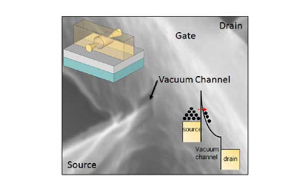
vacuum tubes were the basic components of early electronic devices, by the 1970s they were almost entirely replaced by semiconductor transistors. But in the past few years, researchers have been developing “nanoscale vacuum channel transistors” (NVCTs) that combine the best of vacuum tubes and modern semiconductors into a single device.

Compared to conventional transistors, NVCTs are faster and more resistant to high temperatures and radiation. These advantages make NVCTs ideal candidates for applications such as radiation-tolerant deep space communications, high-frequency devices, and THz electronics. They are also candidates for extending Moore’s law—which states that the number of transistors on a computer chip doubles approximately every two years—which is expected to soon hit a roadblock due to the physical limitations of shrinking semiconductor transistors.
On the other hand, traditional vacuum tubes have certain disadvantages compared to semiconductor transistors, which caused them to become obsolete. Notably, vacuum tubes are very large and consume a lot of energy.
With the new NVCTs, size is no longer an issue because the new devices are produced using modern semiconductor fabrication techniques, and so can be made as small as a few nanometers across. Whereas traditional vacuum tubes look like light bulbs, NVCTs look more like typical semiconductor transistors and can only be seen under a scanning electron microscope.
To address the more pressing issue of energy consumption, in a new study researchers Jin-Woo Han, Dong-Il Moon, and M. Meyyappan at the NASA Ames Research Center in Moffett Field, California, have designed a silicon-based NVCT with an improved gate structure that reduces the drive voltage from tens of volts to less than five volts, resulting in a lower energy consumption. Their work is published in a recent issue of Nano Letters.
In an NVCT, the gate is the component that receives the drive voltage and, based on this voltage, it controls the flow of electrons between two electrodes. In contrast, in the old vacuum tubes, electrons were released by heating the emitter of the device. Because the electrons traveled through a vacuum (the vacuum gap), they moved at very high speeds, which led to the fast operation.
In NVCTs, there is not actually a vacuum, but instead the electrons travel across a space filled with an inert gas such as helium at atmospheric pressure. Since the distance between electrodes is so small (as little as 50 nm), the probability of an electron colliding with a gas molecule is very low, and so the electrons move just as quickly through this “quasi-vacuum” as they do in an actual vacuum. Even with some collisions occurring, the gas molecules are not ionized due to the lower operating voltage.
Perhaps the greatest advantage of the new vacuum transistors is their ability to tolerate high temperatures and ionizing radiation, which makes them promising candidates for the harsh environments often experienced by military and space applications. In the new study, the researchers experimentally demonstrated that the NVCTs continue to operate at the same level of performance at temperatures of up to 200 °C, whereas conventional transistors would cease to function at this temperature. Tests also showed that the new NVCTs are robust against gamma and proton radiation.
In the future, the researchers plan to further improve the performance of this “new old” technology
