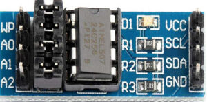
- The AT24C256 EEPROM is an 8-pin, 32-Kbyte EEPROM that stores data and information even when the power is turned off. It works similarly to a pen drive. The information on this IC can be rewritten or retrieved if necessary.
- The AT24C256 EEPROM has a wide operating voltage range of 1.7 to 5.5 volts, making it an ideal EEPROM for both 3.3 and 5-volt systems. This IC has a storage space of 32 Kbytes or 256Kbits and can be expanded by cascading 8 similar EEPROM chips.

- We will first of all try to understand.
- EEPROM (electrically erasable programmable read-only memory) is a non-volatile user-modifiable ROM that allows individual bytes of data to be erased and reprogrammed (written to) repeatedly by applying a higher-than-normal electrical voltage.
- EEPROM uses floating gate or storage transistors to hold a charge and a metal-oxide-silicon (MOS) transistor to erase it. Floating gate transistors (FGTs) are MOS-based complementary bit cells. When the floating gate has no charge, a pulse on the control gate causes the current to flow. At this point, the transistor is operating normally.
- When the gate is charged, it blocks or impedes the control gate’s action, and the current stops flowing. To charge, the source and drain terminals must be grounded, and a sufficient voltage must be applied to the control gate tunnel that runs through the oxide to the floating gate.
- The electrons trapped in the gate determine the charged/uncharged state, which then determines whether the gate’s content is a 0 bit or a 1 bit. A reverse voltage channeled from another transistor dissipates the charge into the substrate, clearing it.
Pin Configuration
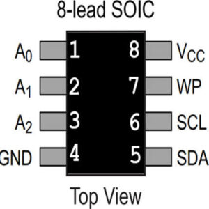
• The pin diagram of AT24C256 EEPROM IC is shown below.

| PIN NO. | PIN NAME | DESCRIPTION |
|---|---|---|
| 1,2,3 | A0,A1,A2 | User configured Chip Select pins, useful during cascading. |
| 4 | GND | Connected to the ground of the circuit. |
| 5 | Serial Data (SDA) | Serial Data pin for I2C Communication. |
| 6 | Serial Clock (SCL) | Serial Clock pin for I2C Communication. |
| 7 | Write-Protect | If connected to GND write is enabled, if connected to Vcc write is disabled. |
| 8 | VCC | Connect to supply rail. |
Working
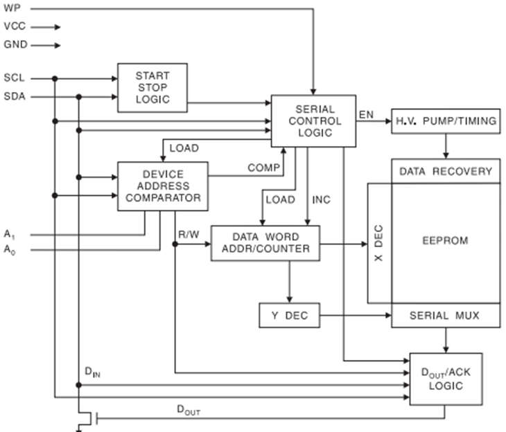
The functional block diagram of AT24C256 EEPROM is shown below.

CLOCK AND DATA TRANSITIONS:
- Normally, the SDA pin is pulled high by an external device. Only during SCL low periods can data on the SDA pin change. Changes in data during SCL high periods indicate a start or stop condition, as defined below.
START CONDITION:
- A start condition is a high-to-low transition of SDA with SCL high that must come before any other command (see Figure 5 on page 9).
STOP CONDITION:
- A stop condition is a low-to-high transition of SDA with SCL high. Following a read sequence, the stop command switches the EEPROM to standby power mode.
ACKNOWLEDGEMENT:
- All addresses and data words are serially transmitted in 8-bit words to and from the EEPROM. During the ninth clock cycle, the EEPROM sends a zero to acknowledge that it has received each word.
- STANDBY MODE: The AT24C128/256 has a low power standby mode that is enabled: a) upon power-up and b) after the STOP bit is received and any internal operations are completed.
MEMORY RESET:
- Any two-wire part can be reset after a protocol interruption, power loss, or system reset by following these steps: (a) Run 9 cycles, (b) look for SDA high in each cycle while SCL is high, and (c) create a start condition while SDA is high.
DEVICE ADDRESSING :
- To enable the chip for a read or write operation, the 128K/256K EEPROM requires an 8-bit device address word following a start condition (see Figure 7 on page 11). The device address word is made up of a one-to-zero sequence for the first five most significant bits, as shown. This is a feature shared by all two-wire EEPROM devices.
- To allow up to four devices on the same bus, the 128K/256K uses the two device address bits A1, and A0. These bits must be compared to their hardwired input pins. If the A1 and A0 pins are allowed to float, an internal proprietary circuit biases them to a logic-low condition.
- The read/write operation select bit is the eighth bit of the device address. If this bit is high, a read operation is started, and if it is low, a write operation is started.
- When the device address is compared, the EEPROM returns a zero. If no comparison is made, the device will go into standby mode.
WRITE OPERATIONS :
- A write operation requires two 8-bit data word addresses following the device address word and acknowledgment. Upon receipt of this address, the EEPROM will again respond with a zero and then clock in the first 8-bit data word. Following receipt of the 8-bit data word, the EEPROM will output a zero. The addressing device, such as a microcontroller, then must terminate the write sequence with a stop condition. At this time the EEPROM enters an internally-timed write cycle, tWR, to the nonvolatile memory. All inputs are disabled during this write cycle and the EEPROM will not respond until the write is complete.
READ OPERATIONS :
- Read operations are initiated the same way as write operations with the exception that the read/write select bit in the device address word is set to one. There are three read operations: current address read, random address read, and sequential read.
