

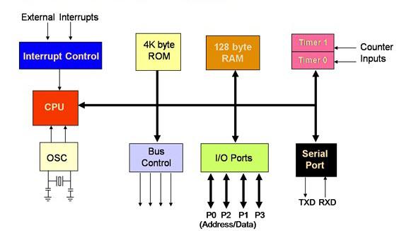
Micro-controllers are widely classify based on their architecture design, storage capacity, processing speed and instruction sets. An 8051 microcontroller is composed of Central Processing Unit, interrupts, memory, ports, timers, serial interface and bus which can study from the architecture. The specialties of this microcontroller are that, it consists of two buses, data units and two memory spaces. The two memories are data memory and program memory, which is helpful in providing sufficient storage for the system.

This 8051-microcontroller is develop by different manufacturers that need to be study before using it in an embedded system. Superior functionalities of 8051-microcontroller have invite its use into multiple application and some are list in the following.

Few Devices Design using 8051-Microcontroller
- Handheld metering systems
- Voltmeter applications
- Safety devices
- Alarming systems
- Instrumentation and controlling systems
- Washing machine and other consumer products
- Energy management systems
- Touch screen
- Adjust engine deviations
Microcontroller are offering the best service for students to enroll themselves into an awesome career opportunity. Our team is compose of faculties with good technical and practical background in the field of hardware as well as software. A project in embedded system using microcontroller requires the knowledge of programming language. Project using 8051 Microcontroller has handled 2000+ projects and define new ideas for associating students with skills.
Features of 8051 Microcontroller
- An 8051 microcontroller comes bundled with the following features −
- 4KB bytes on-chip program memory (ROM)
- 128 bytes on-chip data memory (RAM)
- Four register banks
- 128 user defined software flags
- 8-bit bidirectional data bus
- 16-bit unidirectional address bus
- 32 general purpose registers each of 8-bit
- 16 bit Timers (usually 2, but may have more or less)
- Three internal and two external Interrupts
- Four 8-bit ports,(short model have two 8-bit ports)
- 16-bit program counter and data pointer
- 8051 may also have a number of special features such as UARTs, ADC, Op-amp, etc.
- Block Diagram of 8051 Microcontroller
- The following illustration shows the block diagram of an 8051 microcontroller −
Block Diagram Of 8051 Microcontroller

Digital thermometer using 8051
This article is about a simple 0-100°C digital thermometer with 1°C resolution using 8051. The circuit is based on LM35 analog temperature sensor, ADC0804 and AT89S51 microcontroller. LM35 is an analogue temperature sensor IC which can measure a temperature range of -55 to 150°C. Its output voltage varies 10mV per °C change in temperature.
For example, if the temperature is 32°C, the output voltage will be 32 x 10mV = 320mV. ADC 0804 is used to convert the analogue output voltage of the LM35 to a proportional 8 bit digital value suitable for the microcontroller. The microcontroller accepts the output of ADC, performs necessary manipulations on it and displays it numerically on a 2 digit seven segment LED display.
Out put of the LM35 is connected to the +Vin (pin 6) of the ADC0804. Resistor R13 and preset R14 is used to provide an external reference voltage of 1.28V to the Vref/2 pin ( pin 9) of the ADC0804 and with this reference voltage, the step size of the ADC will be 10mV and span will be 0-1 V. This means that for a 10mV input the digital out of ADC will be 1 (1 in decimal also), for 20mV it will be 10 (2 in decimal), for 30mV it will be 11 (3 in decimal) and so on. The microcontroller accepts this data and puts it on the seven segment display.
Circuit diagram
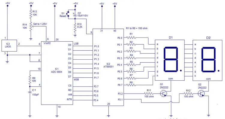

Digital out of the ADC (D0 to D7) are connected to P1 (P1.0 to P1.7) of the microcontroller. This is the line through which the microcontroller accepts data from the ADC. The control pins CS, RD, WR and INTR are connected to P3.7, P3.6, P3.5 and P3.4 of the microcontroller. This is the data path through which the microcontroller sends chip select (CS), read (RD) write (WR) signals to the ADC and receives INTR signal from the ADC. Data lines (a to h) of the multiplexed seven segment display are interfaced to P0 (P0.0 to P0.7) of the microcontroller. Activation signals for the segment driver transistors Q1 and Q2 are available from P3.2 and P3.1 pins of the microcontroller.
Program.
ORG 00H
MOV P1,#11111111B // initializes P1 as input port
MOV P0,#00000000B // initializes P0 as output port
MOV P3,#00000000B // initializes P3 as output port
MOV DPTR,#LABEL // loads the address of “LABEL” to DPTR
MAIN: MOV R4,#250D // loads register R4 with 250D
CLR P3.7 // makes Cs=0
SETB P3.6 // makes RD high
CLR P3.5 // makes WR low
SETB P3.5 // low to high pulse to WR for starting conversion
WAIT: JB P3.4,WAIT // polls until INTR=0
CLR P3.7 // ensures CS=0
CLR P3.6 // high to low pulse to RD for reading the data from ADC
MOV A,P1 // moves the digital output of ADC to accumulator A
MOV B,#10D // load B with 10D
DIV AB // divides the content of A with that in B
MOV R6,A // moves the quotient to R6
MOV R7,B // moves the remainder to R7
DLOOP:SETB P3.2 // sets P3.2 which activates LED segment 1
MOV A,R6 // moves the quotient to A
ACALL DISPLAY // calls DISPLAY subroutine
MOV P0,A // moves the content of A to P0
ACALL DELAY // calls the DELAY subroutine
CLR A // clears A
MOV A,R7 // moves the remainder to A
CLR P3.2 // deactivates LED segment 1
SETB P3.1 // activates LED segment 2
ACALL DISPLAY
MOV P0,A
ACALL DELAY
CLR A
CLR P3.1 // deactivates LED segment 2
DJNZ R4,DLOOP // repeats the loop “DLOOP” until R4=0
SJMP MAIN // jumps back to the main loop
DELAY: MOV R3,#255D // produces around 0.8mS delay
LABEL1: DJNZ R3,LABEL1
RET
DISPLAY: MOVC A,@A+DPTR // converts A’s content to corresponding digit drive pattern
RET
LABEL: DB 3FH // LUT (look up table) starts here
DB 06H
DB 5BH
DB 4FH
DB 66H
DB 6DH
DB 7DH
DB 07H
DB 7FH
DB 6FH
END