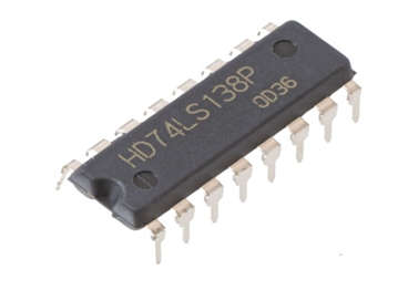
- This IC is a 3 to 8-line decoder or logical decoder IC which is mainly used in the de-multiplexing application.
- The internal circuit of the 74LS138 is built with a high-speed Schottky barrier diode.
- 74LS138 IC is used to decode or demultiplex the application.
- The 74LS138 IC has a 3 input and 8 output pin.

Logical Diagram

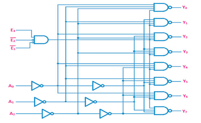
- The logical circuit of this IC is built by using the NOT gate and AND gate.
- This IC has 3 enable pins, 3 input pins, and 8 output pins as shown in the above figure.
Pin Configuration

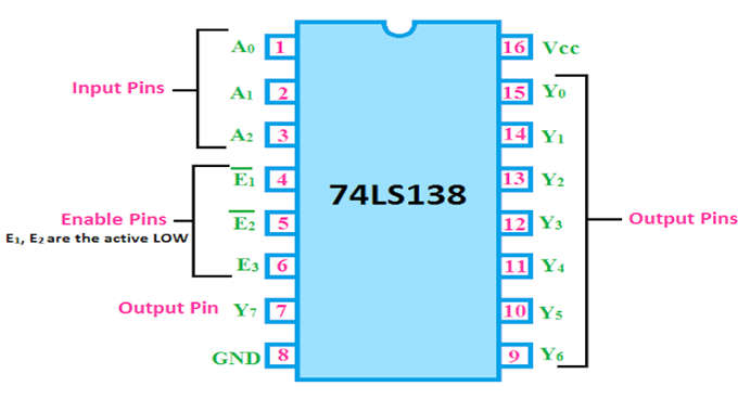
- The above pin diagram shows the pin diagram of 74LS138 IC and the pin description of this IC is shown below.
- 1.Pin (1, 2, 3): This pin is the input pin of this IC (A0, A1, A2).
- 2.Pin (4, 5, 6): This pin is enable pins of this IC (E1, E2, E3), and the E1, and E2 are the active low pins.
- 3.Pin 8: is the GND pin and Pin 16 is the Vcc pin.
- 4.Pin 7 and Pin (9 to 15 ): These pins are output pins (Y0 to Y7).
Truth Table

Applications of 74LS138 IC
- 74LS138 IC is used to decode the digital signal.
- It is used in digital memory circuits.
- This IC is used in data routing applications.
- They are used for demultiplexing of digital signals.
