

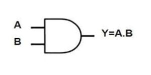
- The 74LS08 is a quadruple 8-bit two-input AND integrated circuit. A gate AND gate is a digital circuit that converts one logic state to another.
- Two logic state signals are used in the AND gate. The first is HIGH, also known as 3-5 Volts, and the second is LOW, also known as 0-2.6 Volts. Two input pins and one output pin are used by a single AND gate.
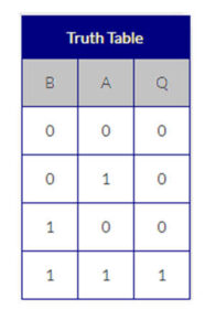
- The output will also be HIGH and LOW, but it will only be HIGH if both input states are HIGH. The single AND gate are simple to construct using transistors, resistors, and diodes.

- First of all, we will understand what is AND gate and what is its function
- The AND gate is an important component of a digital logic circuit. When any of the input states is low, the AND gate’s output state is always low. Simply put, if any input value in the AND gate is set to 0, the output will always be low (0).
- The AND gate’s logic or Boolean expression is the logical multiplication of inputs denoted by a full stop or a single dot as,
A.B=Y - When both inputs A and B are set to true, the value of Y is true.


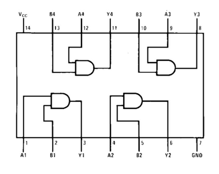
Pin Configurations
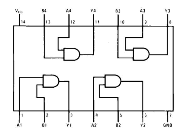


| PINS | FUNCTIONS |
|---|---|
| A1 | Pin 1 will be used as the first input pin for the first AND gate in IC 74LS08. |
| B2 | Pin 2 will be used for the second input pin for the first AND gate in IC 74LS08. |
| Y1 | The output of the first AND gate will be received at Pin 3 |
| A2 | Pin 4 will be used for the first input pin of the second AND gate in IC 74LS08. |
| B2 | Pin 5 will be used to give the second input to the second AND gate in IC 74LS08. |
| Y2 | Pin 6 will be used to receive the output of the second AND gate from IC. |
| GND | Pin 7 is a ground pin; it will be used as common ground by other communication devices with IC and Power Supply. |
| Y3 | Pin 8 will be used to receive the output of the third AND gate from the IC. |
| A3 | Pin 9 will be used to give the first input to the third AND gate to the IC. |
| B3 | Pin 10 will be used to give the second input to the third AND gate to the IC. |
| Y4 | Pin 11 will be used to receive the output of the fourth AND gate from the IC. |
| A4 | Pin 12 will be used as the first input pin of the fourth AND gate. |
| B4 | Pin 13 will be used as the second input pin of the fourth AND gate. |
| VCC | The Power Supply will be provided at pin 14 to make the IC functional. |
Application of 74LS08 AND Gate IC
- The 74LS08 integrated circuit is used to perform general-purpose logic of AND gates.
- The IC has wide use in multiple Digital Systems.
- It is also used in the following devices.
- Digital Electronics.
- Networking Devices.
- Servers.
- Memory Units.
- ALU