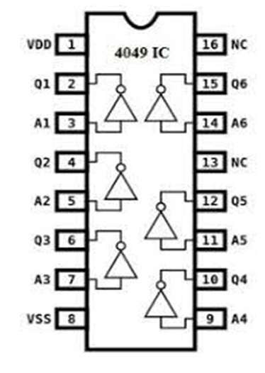
- The IC 4049 consists of six NOT gates inside it and has a high input supply voltage with a maximum current rating of 1mA at 18v.
- 4049 IC is capable to drive two TTL loads.
- We can drive two TTL loads with it. The operating temperature of the IC is -40 to +85 °C. The IC is having high current sink as the input voltage increase the output current sink value will increase, at 15v the current sink value is 26mA.
Pin Configuration
| Number | Pin Name | Description |
|---|---|---|
| 1 | VDD | Positive supply for IC |
| 2 | G | Inverting output 1 for input 1 |
| 3 | A | Input 1 |
| 4 | H | Inverting output 2 for input 2 |
| 5 | B | Input 2 |
| 6 | IN | Inverting output 3 for input 3 |
| 7 | C | Input 3 |
| 8 | VSS | Negative supply for IC |
| 9 | D | Input 4 |
| 10 | J | Inverting output 4 for input 4 |
| 11 | E | Input 5 |
| 12 | K | Inverting output 5 for input 5 |
| 13 | NC | Not connected |
| 14 | F | Input 6 |
| 15 | L | Inverting output 6 for input 6 |
| 16 | NC | not connected |
- CD4049 contains six inverter gates in one package as shown in the diagram.

- In this
- Pin1 is for supply voltage.
- pin3 is input.
- pin2 is for output.
- Pin 5 is the input.
- pin 4 is the output.
- for the second gate similarly, we have four more gates.
- pin 8 is connected to ground.
- Pin 13 and 16 are unused.
Applications of 4049 IC
- Voltage multiplier circuit
- High to low logic converter
- CMOS hex buffer
- Source driver
- CMOS to TTL/DTL Hex converter
