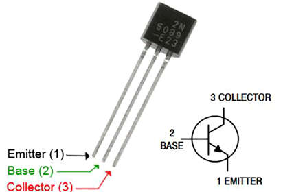
- 2N5089 NPN TRANSISTOR is used for low-level, low-noise amplifier applications.
Pin Configuration

- Pin 1 – Emitter(emits all the free charges).
- Pin 2 – base (transfers all the charges from emitter to collector without/minimum loss).
- Pin 3 – Collector(collects all the charge carriers) produces collector current Ic.
Voltages:
- Collector to Emitter Voltage VCEO = 25 Vdc
- Collector to Base Voltage VCBO = 30 Vdc
- Emitter to Base Voltage VEBO = 3.0 Vdc
Transfer Parameters:
- hFE – Min hFE = 400 (when, IC = 100 Ampdc, VCE = 5.0 Vdc
Max hFE = 1200 (when, IC = 100 Ampdc, VCE = 5.0 Vdc)
Gain:
- Current-gain-bandwidth Product = 50 Mhz
(IC = 500 Adc, VCE = 5.0 Vdc, f = 20 MHz)
Small−Signal Current Gain = 450(min), 1800(max)
Applications of 2N5089 NPN Transistor
- As a switch
- As a low gain amplifier with noise cutoff.
- Push-pull circuits, sensor circuits, low gain amplifiers.