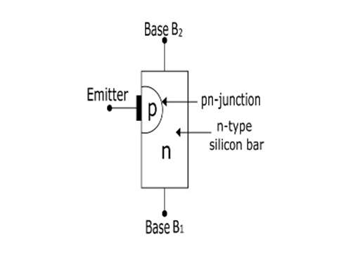
- N2646 is a general-purpose silicon PN Unijunction Transistor that is designed for general-purpose industrial applications.
- This transistor is made out of n-type semiconductors, with the length of the p-type material controlled to help fix the intrinsic standoff ratio parameter. Emitter, base, and collector are the three terminals on a typical 2n2646 UJT.

Pin Configuration
| Pin | Name | Description |
|---|---|---|
| 1 | Base 1 | Normally connected to Power |
| 2 | Emitter | An emitter is used for triggering transistor ON and OFF |
| 3 | Base 2 | Normally connected to Load |
Working
1. When the Emitter is Open
- When the voltage VBB is applied with the emitter open, a potential gradient is established along the n-type silicon bar.
- The voltage V1 (between emitter and B1) establishes a reverse bias on the PN-junction.
- Emitter current is cut off, but a small leakage current flows from B2 to emitter due to minority charge carriers.
- Thus, the device is said to be in an OFF state.
2. With Emitter at Positive Potential
- When a positive voltage is applied at the emitter terminal, the PN-junction will remain reverse biased till the input voltage is less than V1.
- The PN-junction becomes forward-biased when the input voltage at the emitter exceeds V1.
- Under this condition, holes are supplied from the p-type region into the n-type bar, due to this saturation of charge carriers occur.
- The emitter current is limited by the emitter power supply because of this saturation.
- Now, the device is conducting, hence said to be in ON state.
Characteristics of 2N2646 Uni Junction Transistor
- Low Peak Point Current: 5mA (Max).
- Low Emitter Reverse Current:005mA (Typ).
- Maximum voltage between two bases (VB2B1): 35V.
- Maximum emitters reverse voltage (VB2E): 30V.
- Maximum RMS emitter current (Ie): 50mA.
- Maximum peak emitter current (Ie): 2A.
Applications of 2N2646 Uni Junction Transistor
- Timing circuit.
- Voltage detector.
- Phase control circuit.
- General-purpose industrial applications.